FDS6898AZ-F085 Dual N-Channel Logic Level PWM Optimized PowerTrench® MOSFET
FDS6898AZ-F085
Dual N-Channel Logic Level ...
FDS6898AZ-F085 Dual N-Channel Logic Level PWM Optimized PowerTrench®
MOSFET
FDS6898AZ-F085
Dual N-Channel Logic Level PWM Optimized PowerTrench®
MOSFET
General Description
Features
These N-Channel Logic Level
MOSFETs are produced
using
ON
Semiconductor’s
advanced
PowerTrench process that has been especially tailored
to minimize the on-state resistance and yet maintain
superior switching performance.
9.4 A, 20 V
RDS(ON) = 14 mΩ @ VGS = 4.5 V RDS(ON) = 18 mΩ @ VGS = 2.5 V
Low gate charge (16 nC typical)
ESD protection diode (note 3)
These devices are well suited for low
voltage and battery powered applications where low in-line power loss and fast switching are required.
High performance trench technology for extremely low RDS(ON)
High power and current handling capability
Qualified to AEC Q101 RoHS Compliant
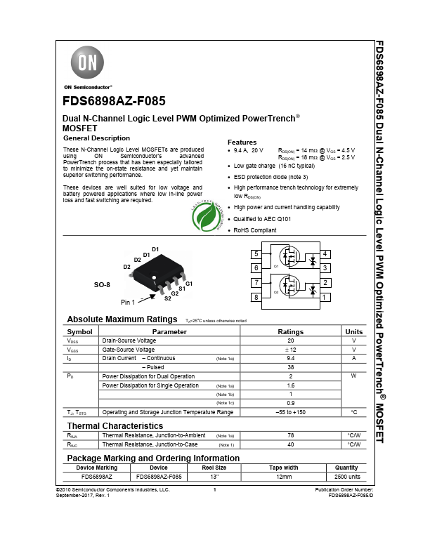
DD2DD1DD1 DD2
SO-8
Pin 1 SO-8
SS2GS2SS1GG1
5
4
6
Q1
3
7
2
Q2
8
1
Absolute Maximum Ratings TA=25oC unless otherwise noted
Symbol
VDSS VGSS ID
PD
Parameter
Drain-Source
Voltage Gate-Source
Voltage Drain Current – Continuous
– Pulsed Power Dissipation for Dual Operation Power Dissipation for Single Operation
(Note 1a) (Note 1a)
(Note 1b)
(Note 1c)
TJ, TSTG
Operating and Storage Junction Temperature Range
Thermal Characteristics
RθJA
Thermal Resistance, Junction-to-Ambient
RθJC
Thermal Resistance, Junction-to-Case
(Note 1a) (Note 1)
Package Marking and Ordering Information
Device Marking
Device
Reel Size
FDS689...