FDS6984AS
J
May 2008
FDS6984AS
General Description
Dual Notebook Power Supply N-Channel PowerTrench® SyncFET™
Feature...
FDS6984AS
J
May 2008
FDS6984AS
General Description
Dual Notebook Power Supply N-Channel PowerTrench® SyncFET™
Features
Q2: Optimized to minimize conduction losses Includes SyncFET Schottky diode RDS(on) max= 20 mΩ @ VGS = 10V RDS(on) max= 28 mΩ @ VGS = 4.5V Q1: Optimized for low switching losses Low gate charge (8nC typical) RDS(on) max= 31 mΩ @ VGS = 10V RDS(on) max= 40 mΩ @ VGS = 4.5V RoHS Compliant The FDS6 984AS is designed t o replace t wo single SO-8 MOS FETs and Schottk y diode in s ynchronous DC:DC p ower supplies that prov ide various perip heral
voltages for not ebook computer s and oth er battery powered electro nic devices . FDS6984AS contains tw o unique 30V, N-channel, logic level, PowerT rench
MOSFETs designed to maximi ze pow er conversion efficiency. The high-side sw itch ( Q1) is designed w ith sp ecific emphasis on reducing sw itching losse s w hile th e low side sw itch (Q2 ) is optimized t o reduce condu ction losses. Q2 also includes a pate nted combination of a
MOSFET mono lithically integrat ed w ith a Schottk y diode.
8.5A, 30V
5.5A, 30V
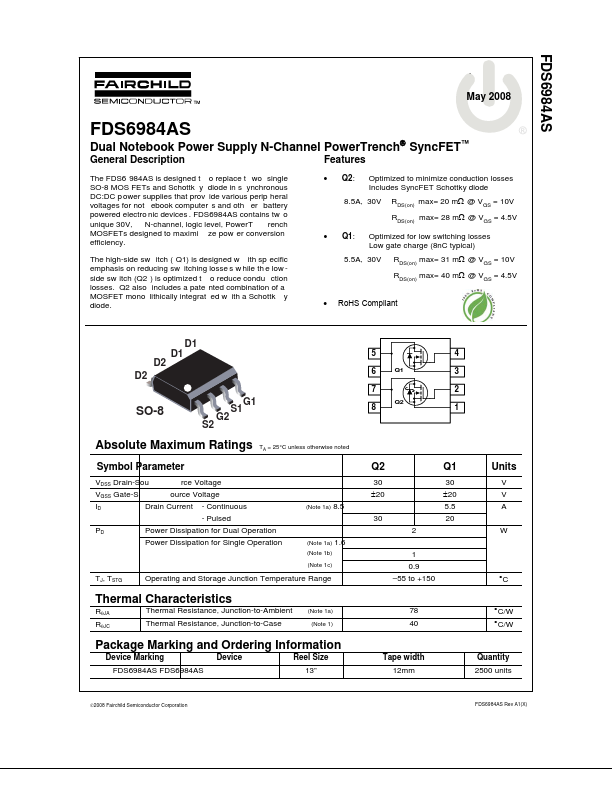
D1 D1 D2 D2 S1 G1
5 6 7
Q1
4 3 2
Q2
SO-8
S2
8
1
G2
Absolute Maximum Ratings
Symbol Parameter
VDSS Drain-Sou VGSS Gate-S ID PD rce
Voltage ource
Voltage
TA = 25°C unless otherwise noted
Q2
30 ±20
(Note 1a)
Q1
30 ±20 5.5 20 2
Units
V V A W
- Continuous - Pulsed Power Dissipation for Dual Operation Power Dissipation for Single Operation
Drain Current
8.5 30
(Note 1a) (Note 1b) (Note 1c)
1.6 1 0...