FDS7066ASN3
August 2004
FDS7066ASN3
30V N-Channel PowerTrench® SyncFET™
General Description
The FDS7066ASN3 is designe...
FDS7066ASN3
August 2004
FDS7066ASN3
30V N-Channel PowerTrench® SyncFET™
General Description
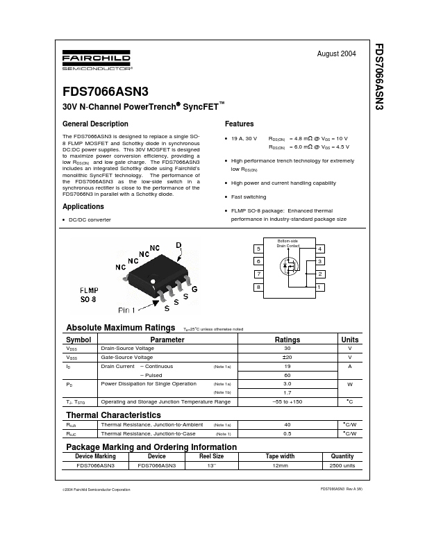
The FDS7066ASN3 is designed to replace a single SO8 FLMP
MOSFET and Schottky diode in synchronous DC:DC power supplies. This 30V
MOSFET is designed to maximize power conversion efficiency, providing a low RDS(ON) and low gate charge. The FDS7066ASN3 includes an integrated Schottky diode using Fairchild’s monolithic SyncFET technology. The performance of the FDS7066ASN3 as the low-side switch in a synchronous rectifier is close to the performance of the FDS7066N3 in parallel with a Schottky diode.
Features
19 A, 30 V RDS(ON) = 4.8 mΩ @ VGS = 10 V RDS(ON) = 6.0 mΩ @ VGS = 4.5 V High performance trench technology for extremely low RDS(ON) High power and current handling capability Fast switching FLMP SO-8 package: Enhanced thermal performance in industry-standard package size
Applications
DC/DC converter
5 6 7 8
Bottom-side Drain Contact
4 3 2 1
Absolute Maximum Ratings
Symbol
VDSS VGSS ID PD TJ, TSTG Drain-Source
Voltage Gate-Source
Voltage Drain Current – Continuous – Pulsed
TA=25oC unless otherwise noted
Parameter
Ratings
30 ±20
(Note 1a)
Units
V V A W °C
19 60 3.0 1.7 –55 to +150
Power Dissipation for Single Operation
(Note 1a) (Note 1b)
Operating and Storage Junction Temperature Range
Thermal Characteristics
RθJA RθJC Thermal Resistance, Junction-to-Ambient Thermal Resistance, Junction-to-Case
(Note 1a) (Note 1)
40 0.5
°C/W °C/W
Package Marking and Ord...