FDS9933BZ Dual P-Channel 2.5V Specified PowerTrench® MOSFET
March 2008
FDS9933BZ
Dual P-Channel 2.5V Specified PowerTr...
FDS9933BZ Dual P-Channel 2.5V Specified PowerTrench®
MOSFET
March 2008
FDS9933BZ
Dual P-Channel 2.5V Specified PowerTrench®
MOSFET
tm
-20V, -4.9A, 46mΩ
Features
General Description
Max rDS(on) = 46mΩ at VGS = -4.5V, ID = -4.9A Max rDS(on) = 69mΩ at VGS = -2.5V, ID = -4.0A Low gate charge (11nC typical). High performance trench technology for extremely low rDS(on). HBM ESD protection level >3kV (Note 3). RoHS Compliant
These P-Channel 2.5V specified
MOSFETs are produced using Fairchild Semiconductor’s advanced PowerTrench® process that has been especially tailored to minimize the on-state resistance and yet maintain low gate charge for superior switching performance.
These devices are well suited for portable electronics applications: load switching and power management, battery charging and protection circuits.
Applications
Battery Charging Load Switching
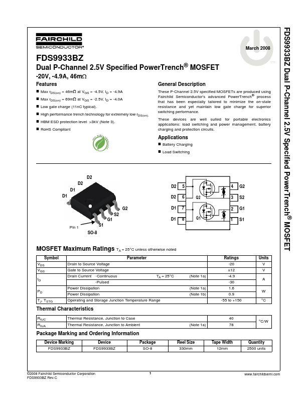
D2 D2 D1 D1
Pin 1
G2 S2 G1 S1
SO-8
D2 5 D2 6 D1 7 D1 8
Q 12 Q 21
4 G2 3 S2 2 G1 1 S1
MOSFET Maximum Ratings TA = 25°C unless otherwise noted
Symbol VDS VGS ID
PD TJ, TSTG
Parameter
Drain to Source
Voltage
Gate to Source
Voltage
Drain Current -Continuous -Pulsed
TA = 25°C
Power Dissipation
Power Dissipation
Operating and Storage Junction Temperature Range
Thermal Characteristics
(Note 1a)
(Note 1a) (Note 1b)
Ratings -20 ±12 -4.9 -30 1.6 0.9
-55 to +150
Units V V A
W °C
RθJC RθJA
Thermal Resistance, Junction to Case Thermal Resistance, Junction to Ambient
Package Marking and Orde...