Transistor, N-Channel, Field Effect, Enhancement Mode
FDT457N
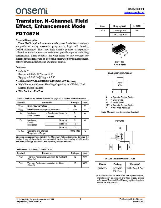
General Description These N−Channel enhancement mode power...
Transistor, N-Channel, Field Effect, Enhancement Mode
FDT457N
General Description These N−Channel enhancement mode power field effect transistors
are produced using onsemi’s proprietary, high cell density, DMOS technology. This very high density process is especially tailored to minimize on−state resistance, provide superior switching performance. These products are well suited to low
voltage, low current applications such as notebook computer power management, battery powered circuits, and DC motor control.
Features
5 A, 30 V
RDS(on) = 0.06 W @ VGS = 10 V RDS(on) = 0.090 W @ VGS = 4.5 V
High Density Cell Design for Extremely Low RDS(ON) High Power and Current Handling Capability in a Widely Used
Surface Mount Package
This Device is Pb−Free
ABSOLUTE MAXIMUM RATINGS (TA = 25°C unless otherwise noted)
Symbol
Parameter
Ratings Unit
VDSS Drain−Source
Voltage
30
V
VGSS Gate−Source
Voltage − Continuous
±20
V
ID
Maximum
− Continuous (Note 1a)
5
A
Drain Current
− Pulsed
16
PD
Maximum
Power
Dissipation
(Note 1a)
3
W
(Note 1b)
1.3
(Note 1c)
1.1
TJ, Tstg Operating and Storage Temperature Range
−65 to +150 °C
Stresses exceeding those listed in the Maximum Ratings table may damage the device. If any of these limits are exceeded, device functionality should not be assumed, damage may occur and reliability may be affected.
THERMAL CHARACTERISTICS
Symbol
Parameter
RqJA
Thermal Resistance, Junction−to−Ambient (Note 1a)
RqJC
Thermal Resistance, Ju...