n-channel JFETs
designed for • • •
• Analog Switches • Commutators • Choppers • Integrator Reset Switch
*ABSOLUTE MAXIMU...
n-channel JFETs
designed for
Analog Switches Commutators Choppers Integrator Reset Switch
*ABSOLUTE MAXIMUM RATINGS (25°C)
Reverse Gate-Drain or Gate-Source
Voltage ___ ..... _-40 V Gate Current ............... _........... _.... 50 rnA Total Device Dissipation at 25°C Case Temperature
(Derate 10 mW;oC) ..... , ____ .. _............. 1.8 W Storage Temperature Range. _... _........ --65 to +200°C Lead Temperature
(1/16" from case for 60 seconds) ...............300°C
H
Siliconix
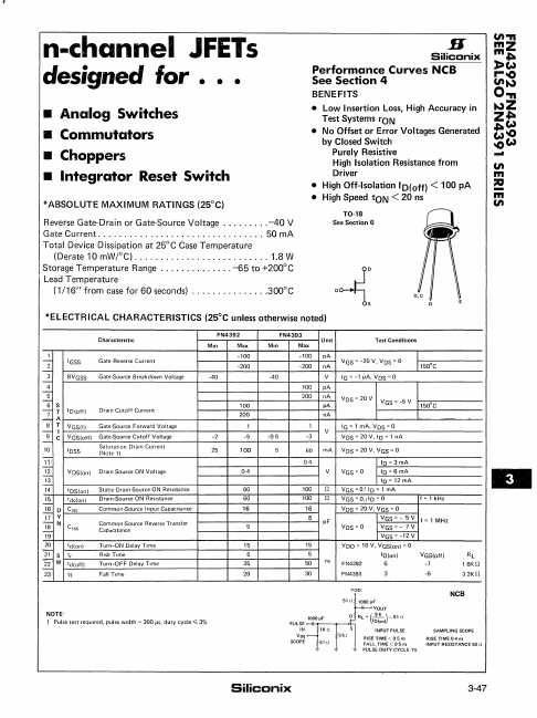
Performance Curves NCB See Section 4
BENEFITS
Low Insertion Loss, High Accuracy in Test Systems rON
No Offset or Error
Voltages Generated by Closed Switch
Purely Resistive
High Isolation Resistance from
Driver
High Off-Isolation ID(off) < 100 pA High Speed tON < 20 ns
TO-18 See Section 6
Q
-'m~"
m
'"
o~: o5
*ELECTRICAL CHARACTERISTICS (25°C unless otherwise noted)
Characteristic
'.--....432!..
IGSS 8VGSS
5
~S
]T IDloff)
I---, .A
81 T
Ig-
'I
c,
VGSlfi VGSloff)
~
10 IDSS
1ii
-~1:3- VDSlon)
14 rOSlon)
-15 rds(on)
.g~ D CISS
Y
18 ~
N
C rss
20 tdlon)
"'21 s t,
-~22 ' W tdloff)
23 tf
Gate Reverse Current
Gate-Source Breakdown
Voltage
Drain Cutoff Current
Gate-Source Forward
Voltage Gate-Source Cutoff
Voltage Saturation Dram Current
INot.1I
Dram Source ON
Voltage
Static Dram-Source ON Resistance Dram-Source ON Resistance Common-Source Input Capacitance Common-Source Reverse Transfer Capdcltance Turn-ON Delay Time Rise Time Turn-OFF Delay Time Fall Time
FN4...