FQD12P10TM_F085 P-Channel MOSFET
February 2010
FQD12P10TM_F085
100V P-Channel MOSFET
General Description
These P-Chann...
FQD12P10TM_F085 P-Channel
MOSFET
February 2010
FQD12P10TM_F085
100V P-Channel
MOSFET
General Description
These P-Channel enhancement mode power field effect transistors are produced using Fairchild’s proprietary, planar stripe, DMOS technology. This advanced technology has been especially tailored to minimize on-state resistance, provide superior switching performance, and withstand high energy pulse in the avalanche and commutation mode. These devices are well suited for low
voltage applications such as audio amplifier, high efficiency switching DC/DC converters, and DC motor control.
Features
-9.4A, -100V, RDS(on) = 0.29Ω @VGS = -10 V Low gate charge ( typical 21 nC) Low Crss ( typical 65 pF) Fast switching 100% avalanche tested Improved dv/dt capability
Qualified to AEC Q101
RoHS Compliant
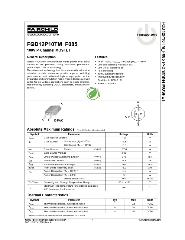
tm
DD
G S D-PAK
Absolute Maximum Ratings TC = 25°C unless otherwise noted
Symbol VDSS ID
IDM VGSS EAS IAR EAR dv/dt PD
TJ, TSTG TL
Parameter
Drain-Source
Voltage
Drain Current
- Continuous (TC = 25°C) - Continuous (TC = 100°C)
Drain Current - Pulsed
(Note 1)
Gate-Source
Voltage
Single Pulsed Avalanche Energy
(Note 2)
Avalanche Current
(Note 1)
Repetitive Avalanche Energy
(Note 1)
Peak Diode Recovery dv/dt Power Dissipation (TA = 25°C) * Power Dissipation (TC = 25°C)
- Derate above 25°C
(Note 3)
Operating and Storage Temperature Range
Maximum lead temperature for soldering purposes, 1/8! from case for 5 seconds
Thermal Characteristics
Symbol RθJC...