FQP7N65/FQPF7N65
650V, 7A N-Channel MOSFET
General Description
Product Summary
The FQP7N65 & FQPF7N65 have been fabri...
FQP7N65/FQPF7N65
650V, 7A N-Channel
MOSFET
General Description
Product Summary
The FQP7N65 & FQPF7N65 have been fabricated using an advanced high
voltage MOSFET process that is designed to deliver high levels of performance and robustness in popular AC-DC applications. By providing low RDS(on), Ciss and Crss along with guaranteed avalanche capability these parts can be adopted quickly into new and existing offline power supply designs.
VDS ID (at VGS=10V) RDS(ON) (at VGS=10V)
100% UIS Tested 100% Rg Tested
750V@150℃ 7A < 1.56Ω
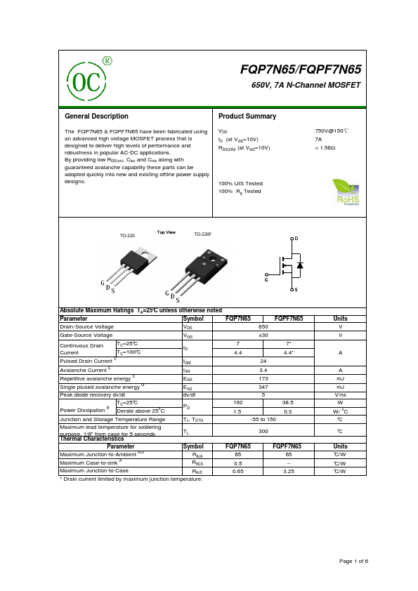
TO-220
Top View
TO-220F
D
G S
Absolute Maximum Ratings TA=25°C unless otherwise noted
Parameter
Symbol
FAQOPT7N65
FAQOPTF7N65
Drain-Source
Voltage
VDS 650
Gate-Source
Voltage
VGS ±30
Continuous Drain
TC=25°C
Current
TC=100°C
Pulsed Drain Current C
Avalanche Current C
Repetitive avalanche energy C
Single plused avalanche energy G
Peak diode recovery dv/dt
ID
IDM IAR EAR EAS dv/dt
7 7* 4.4 4.4*
24 3.4 173 347 5
TC=25°C Power Dissipation B Derate above 25oC
PD
192 38.5 1.5 0.3
Junction and Storage Temperature Range
Maximum lead temperature for soldering purpose, 1/8" from case for 5 seconds Thermal Characteristics
TJ, TSTG TL
-55 to 150 300
Parameter Maximum Junction-to-Ambient A,D
Maximum Case-to-sink A
Symbol RθJA RθCS
FQP7N65 65 0.5
FQPF7N65 65 --
Maximum Junction-to-Case
RθJC
* Drain current limited by maximum junction temperature.
0.65
3.25
Units V V
A
A mJ mJ V/ns W W/ oC °C
°C
Units °C/W °C/W °C/W
Page ...