DATA SHEET www.onsemi.com
FSUSB242 Type-C USB Port Protection Switch
FSUSB242UCX-Z002
Features
• Fully USB Data Port P...
DATA SHEET www.onsemi.com
FSUSB242 Type-C USB Port Protection Switch
FSUSB242UCX-Z002
Features
Fully USB Data Port Protection VDD 0 V− 5.5 V (12 V DC tolerant) −18 V to +20 V DC Tolerance on HSD± Port ±25 V IEC 61000−4−5 Surge Protection w/o External TVS VDD Operating Range, 2.7 V−5.5 V HSD RON: 5 W Typical CON = 5 pF Typical Wide −3 dB Bandwidth: > 720 MHz Low Power Operation: ICC < 10 mA (Typical) Over
Voltage Protection: 3.6 V & 4.5 V
Typical Applications
Smartphones Tablets Laptops
Safety Mechanisms Highlight
3.6 V & 4.5 V OVP Trip Point ±25 V Surge Protection without Need for External TVS
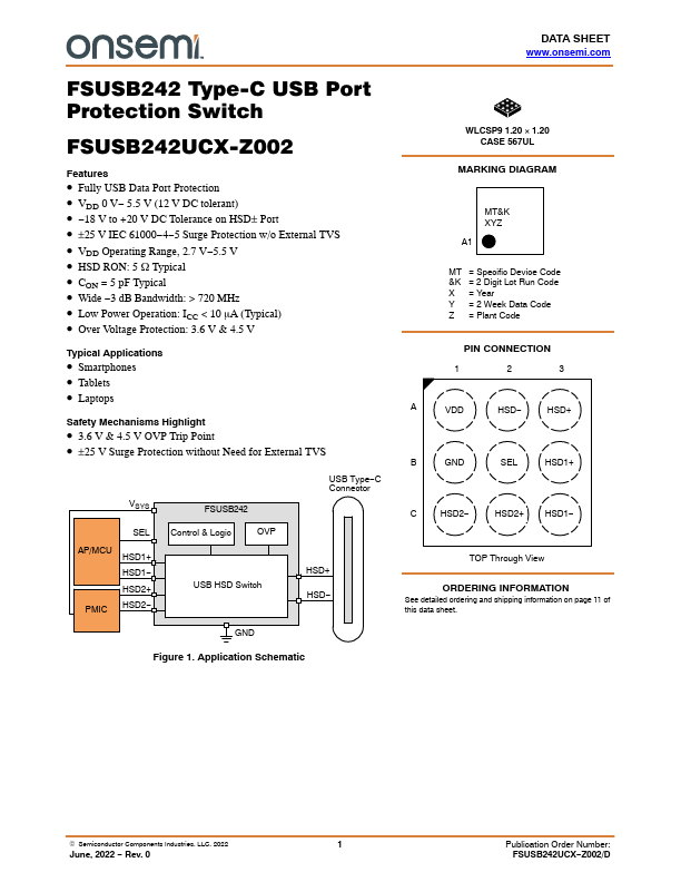
VSYS
SEL AP/MCU
HSD1+ HSD1− HSD2+ PMIC HSD2−
FSUSB242
Control & Logic
OVP
USB HSD Switch
USB Type−C Connector
HSD+ HSD−
GND
Figure 1. Application Schematic
WLCSP9 1.20 y 1.20 CASE 567UL
MARKING DIAGRAM
MT&K XYZ
A1
MT = Specific Device Code &K = 2 Digit Lot Run Code X = Year Y = 2 Week Data Code Z = Plant Code
PIN CONNECTION
1
2
3
A
VDD
HSD−
HSD+
B
GND
SEL
HSD1+
C
HSD2−
HSD2+ HSD1−
TOP Through View
ORDERING INFORMATION
See detailed ordering and shipping information on page 11 of this data sheet.
© Semiconductor Components Industries, LLC, 2022
1
June, 2022 − Rev. 0
Publication Order Number: FSUSB242UCX−Z002/D
FSUSB242UCX−Z002
VDD
SEL
Control & Logic OVP
HSD1+
HSD2+ HSD1−
HSD2−
HSD+ HSD−
GND Figure 2. Simplified Block Diagram
Table 1. PIN FUNCTION DESCRIPTION
CSP Bump
Name
A1
VDD
B1
GND
A3
HSD+
A2
HSD−
B3
HSD...