www.DataSheet4U.com
Pb Free Plating Product
ISSUED DATE :2005/06/09 REVISED DATE :
G3403A
P-CHANNEL ENHANCEMENT MODE P...
www.DataSheet4U.com
Pb Free Plating Product
ISSUED DATE :2005/06/09 REVISED DATE :
G3403A
P-CHANNEL ENHANCEMENT MODE POWER
MOSFET
BVDSS RDS(ON) ID
-30V 70m -3.2A
The G3403A provide the designer with best combination of fast switching, low on-resistance and cost-effectiveness. The G3403A is universally preferred for all commercial-industrial surface mount applications and suited for low
voltage applications such as DC/DC converters.
Description
Features
*Simple Drive Requirement *Small Package Outline
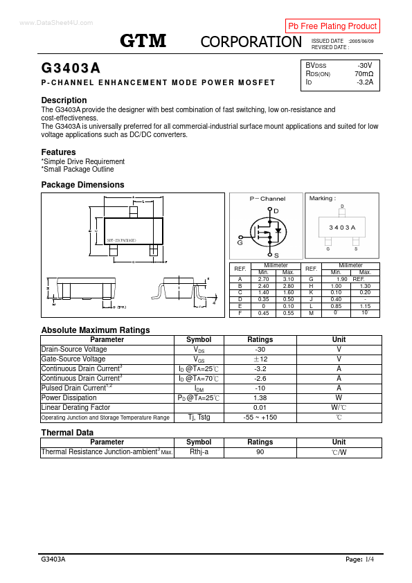
Package Dimensions
REF. A B C D E F
Millimeter Min. Max. 2.70 3.10 2.40 2.80 1.40 1.60 0.35 0.50 0 0.10 0.45 0.55
REF. G H K J L M
Millimeter Min. Max. 1.90 REF. 1.00 1.30 0.10 0.20 0.40 0.85 1.15 0 10
Absolute Maximum Ratings
Parameter Drain-Source
Voltage Gate-Source
Voltage Continuous Drain Current3 Continuous Drain Current3 Pulsed Drain Current1,2 Power Dissipation Linear Derating Factor
Operating Junction and Storage Temperature Range
Symbol VDS VGS ID @TA=25 ID @TA=70 IDM PD @TA=25 Tj, Tstg Symbol Rthj-a
Ratings -30 12 -3.2 -2.6 -10 1.38 0.01 -55 ~ +150 Ratings 90
Unit V V A A A W W/
Thermal Data
Parameter 3 Thermal Resistance Junction-ambient Max. Unit /W
1/4
ISSUED DATE :2005/06/09 REVISED DATE :
Electrical Characteristics(Tj = 25
Parameter Drain-Source Breakdown
Voltage
Breakdown
Voltage Temperature Coefficient
Unless otherwise specified)
Min. -30 -0.5 Typ. -0.1 9 10 1.8 3.6 7 15 21 15 735 100 80 Max. -1.2 100 -1 -25 70 85 120 18 1325 pF ns nC m Uni...