GM BT3019
Description Package Dimensions
1/1 NP N E PITAXI AL P L ANAR T RANS ISTO R
The GMBT3019 is designed for gene...
GM BT3019
Description Package Dimensions
1/1 NP N E PITAXI AL P L ANAR T RANS ISTO R
The GMBT3019 is designed for general purpose amplifier applications and switching requiring collector currents 1A.
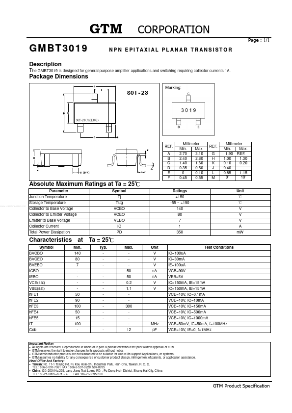
REF. A B C D E F
Millimeter Min. Max. 2.70 3.10 2.40 2.80 1.40 1.60 0.35 0.50 0 0.10 0.45 0.55
REF. G H K J L M
Millimeter Min. Max. 1.90 REF. 1.00 1.30 0.10 0.20 0.40 0.85 1.15 0 10 Unit
Absolute Maximum Ratings at Ta = 25
Parameter Junction Temperature
www.DataSheet4U.com
Symbol Tj Tstg VCBO VCEO VEBO IC PD
Ratings +150 -55 ~ +150 140 80 7 1 350
Storage Temperature Collector to Base
Voltage Collector to Emitter
Voltage Emitter to Base
Voltage Collector Current Total Power Dissipation
V V V A mW
Characteristics
Symbol BVCBO BVCEO BVEBO ICBO IEBO VCE(sat) VBE(sat) hFE1 hFE2 hFE3 hFE4 hFE5 fT Cob
at Ta = 25
Min. 140 80 7 50 90 100 50 15 100 Typ. Max. 50 50 0.2 1.1 300 12 MHz pF Unit V V V nA nA V V IC=100uA IC=30mA IE=100uA VCB=90V VEB=5V IC=150mA, IB=15mA IC=150mA, IB=15mA VCE=10V, IC=0.1mA VCE=10V, IC=10mA VCE=10V, IC=150mA VCE=10V, IC=500mA VCE=10V, IC=1000mA VCE=50mV, IC=50mA, f=100MHz VCE=10V, IE=0, f=1MHz Test Conditions
Important Notice: All rights are reserved. Reproduction in whole or in part is prohibited without the prior written approval of GTM. GTM reserves the right to make changes to its products without notice. GTM semiconductor products are not warranted to be suitable for use in life-support Applications, or systems. GTM assumes no liability for any...