Features
■ Low forward voltage drop ■ Fast switching ■ PN junction guard ring for transient and ESD protection
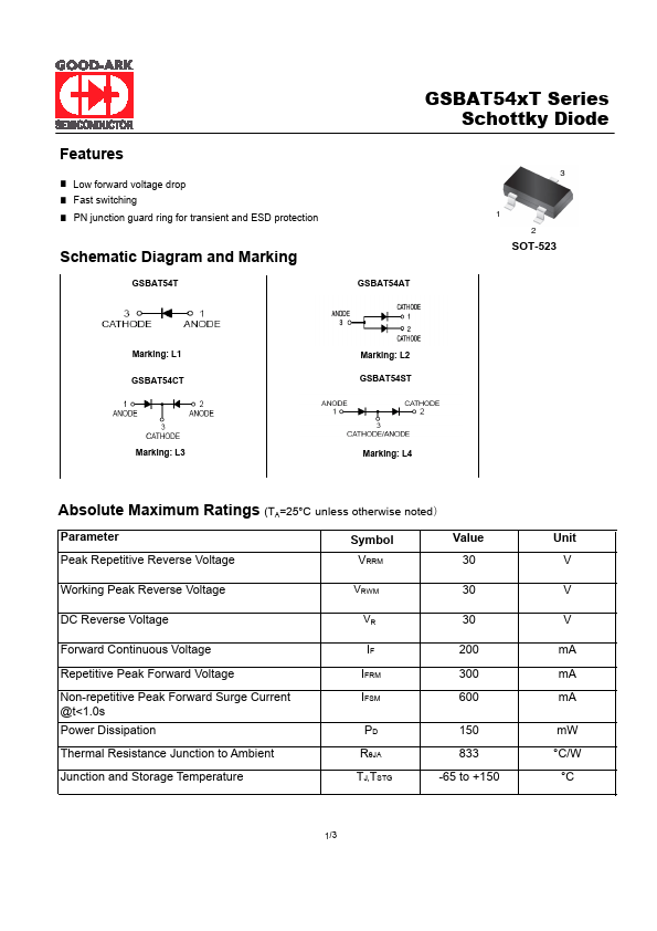
Schematic...
Features
■ Low forward
voltage drop ■ Fast switching ■ PN junction guard ring for transient and ESD protection
Schematic Diagram and Marking
GSBAT54T
GSBAT54xT Series Schottky Diode
GSBAT54AT
3
1 2
SOT-523
Marking: L1 GSBAT54CT
Marking: L2 GSBAT54ST
Marking: L3
Marking: L4
Absolute Maximum Ratings (TA=25°C unless otherwise noted)
Parameter Peak Repetitive Reverse
Voltage
Symbol VRRM
Value 30
Working Peak Reverse
Voltage
VRWM
30
DC Reverse
Voltage
VR 30
Forward Continuous
Voltage
Repetitive Peak Forward
Voltage
Non-repetitive Peak Forward Surge Current @t<1.0s Power Dissipation
Thermal Resistance Junction to Ambient
Junction and Storage Temperature
IF IFRM IFSM
PD RθJA TJ,TSTG
200 300 600
150 833 -65 to +150
1/3
Unit V
V
V
mA mA mA
mW °C/W
°C
GSBAT54xT Series Schottky Diode
Electrical Characteristics (TA=25°C unless otherwise noted)
Parameter
Symbol Test Conditions
Reverse Breakdown
Voltage V(BR)R
IR=100μA
Leakage Current Forward
Voltage
=IR VR 25V
IF=0.1mA IF=1.0mA VF IF=10mA IF=30mA
Min Max
30
2.0 240 320 400 500
Unit V μA
mV
Typical Total Capacitance =CT =VR 1.0V,f 1MHz
Reverse Recovery Time
trr
IF=IR=10mA,to IR=1.0mA RL=100Ω
10 pF 5.0 ns
Typical Electrical Characteristic Curves
1/3
2/3
Package Outline Dimensions
A
KB
D G
H
SOT-523
C
J
GSBAT54xT Series Schottky Diode
SOT-523
Dim Min Max A 1.5 1.7 B 0.75 0.85 C 0.6 0.8 D 0.15 0.3 G 0.9 1.1 H 0.02 0.1 J 0.1Typical K 1.45 1.75 All Dimensions in mm
www.goodarksemi.com
3/3 Doc.USGSB...