GSDAN222 Switching Diode
Features
■ High speed ■ Suitable for high packing density layout ■ High reliability
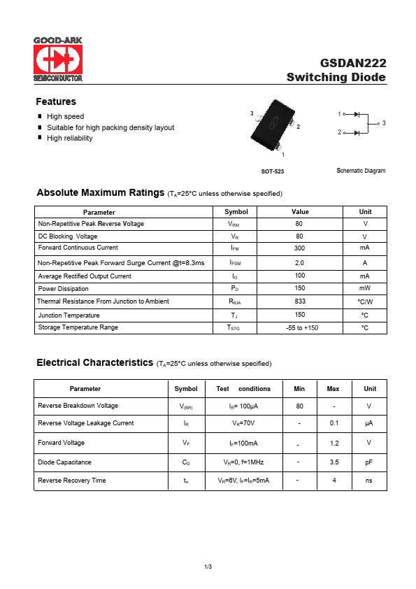
3 2
1 SOT...
GSDAN222 Switching Diode
Features
■ High speed ■ Suitable for high packing density layout ■ High reliability
3 2
1 SOT-523
Absolute Maximum Ratings (TA=25°C unless otherwise specified)
Parameter Non-Repetitive Peak Reverse
Voltage DC Blocking
Voltage Forward Continuous Current
Non-Repetitive Peak Forward Surge Current @t=8.3ms Average Rectified Output Current Power Dissipation Thermal Resistance From Junction to Ambient
Junction Temperature Storage Temperature Range
Symbol VRM VR IFM
IFSM IO PD RθJA
TJ TSTG
Value 80 80 300
2.0 100 150 833 150 -55 to +150
1 3
2
Schematic Diagram
Unit V V
mA A mA mW °C/W °C °C
Electrical Characteristics (TA=25°C unless otherwise specified)
Parameter Reverse Breakdown
Voltage Reverse
Voltage Leakage Current Forward
Voltage Diode Capacitance Reverse Recovery Time
Symbol
Test conditions
Min
Max
V(BR)
IR= 100μA
80 -
IR VR=70V - 0.1
VF IF=100mA -
CD VR=0, f=1MHz -
trr
VR=6V, IF=IR=5mA
-
1.2 3.5 4
Unit V μA V pF ns
1/3
T a
=100℃
Typical Characteristics Curves
Forward Characteristics
300 100
10
1
T a
=25℃
GSDAN222 Switching Diode
10000 1000 100 10
Reverse Characteristics
T =100℃ a
T =25℃ a
REVERSE CURRENT I (nA) R
FORWARD CURRENT I (mA) F
0.1 0.0
0.4 0.8 1.2
FORWARD
VOLTAGE V (V) F
1.6
1 0 20 40 60 80
REVERSE
VOLTAGE V (V) R
CAPACITANCE BETWEEN TERMINALS C (pF)
T
POWER DISSIPATION P (mW) D
Capacitance Characteristics
1.6 T =25℃
a
f=1MHz 1.4
1.2
1.0
0.8
0.6 0 4 8 12 16 20
REVERSE
VOLTAGE V (V) R
Power Derating ...