www.DataSheet4U.com
ISSUED DATE :2005/08/31 REVISED DATE :
G S M B TA 0 5
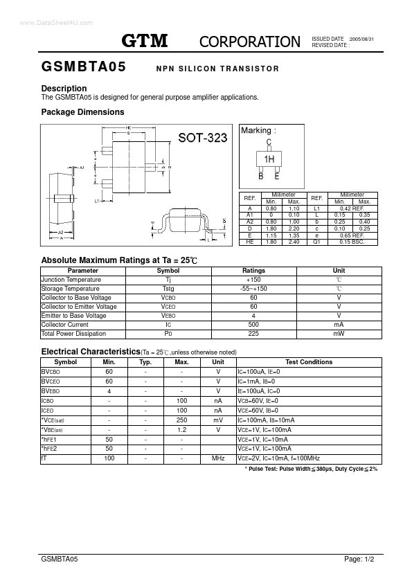
Description Package Dimensions
NPN SILICON T...
www.DataSheet4U.com
ISSUED DATE :2005/08/31 REVISED DATE :
G S M B TA 0 5
Description Package Dimensions
NPN SILICON TRANSISTOR
The GSMBTA05 is designed for general purpose amplifier applications.
REF. A A1 A2 D E HE
Millimeter Min. Max. 0.80 1.10 0 0.10 0.80 1.00 1.80 2.20 1.15 1.35 1.80 2.40
REF. L1 L b c e Q1
Millimeter Min. Max. 0.42 REF. 0.15 0.35 0.25 0.40 0.10 0.25 0.65 REF. 0.15 BSC.
Absolute Maximum Ratings at Ta = 25
Parameter Junction Temperature Storage Temperature Collector to Base
Voltage Collector to Emitter
Voltage Emitter to Base
Voltage Collector Current Total Power Dissipation Symbol Tj Tstg VCBO VCEO VEBO IC PD ,unless otherwise noted) Max. 100 100 250 1.2 MHz Unit V V V nA nA mV V IC=100uA, IE=0 IC=1mA, IB=0 IE=100uA, IC=0 VCB=60V, IE=0 VCE=60V, IB=0 IC=100mA, IB=10mA VCE=1V, IC=100mA VCE=1V, IC=10mA VCE=1V, IC=100mA VCE=2V, IC=10mA, f=100MHz
* Pulse Test: Pulse Width 380 s, Duty Cycle 2%
Ratings +150 -55~+150 60 60 4 500 225
Unit
V V V mA mW
Electrical Characteristics(Ta = 25
Symbol BVCBO BVCEO BVEBO ICBO ICEO *VCE(sat) *VBE(on) *hFE1 *hFE2 fT Min. 60 60 4 50 50 100 Typ. -
Test Conditions
GSMBTA05
Page: 1/2
ISSUED DATE :2005/08/31 REVISED DATE :
Characteristics Curve
Important Notice: All rights are reserved. Reproduction in whole or in part is prohibited without the prior written approval of GTM. GTM reserves the right to make changes to its products without notice. GTM semiconductor products are not warranted to be suitable for use in...