GT40T302
TOSHIBA Insulated Gate Bipolar Transistor Silicon N Channel IGBT
GT40T302
Parallel Resonance Inverter Switchin...
GT40T302
TOSHIBA Insulated Gate Bipolar Transistor Silicon N Channel IGBT
GT40T302
Parallel Resonance Inverter Switching Applications
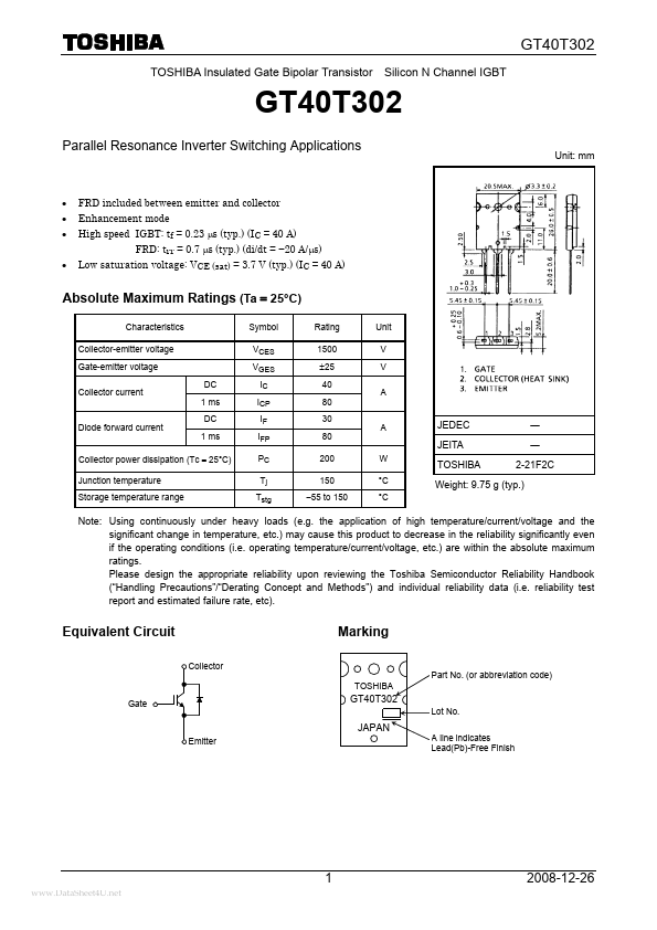
Unit: mm FRD included between emitter and collector Enhancement mode High speed IGBT: tf = 0.23 μs (typ.) (IC = 40 A) FRD: trr = 0.7 μs (typ.) (di/dt = −20 A/μs) Low saturation
voltage: VCE (sat) = 3.7 V (typ.) (IC = 40 A)
Absolute Maximum Ratings (Ta = 25°C)
Characteristics Collector-emitter
voltage Gate-emitter
voltage Collector current DC 1 ms DC 1 ms Symbol VCES VGES IC ICP IF IFP PC Tj Tstg Rating 1500 ±25 40 80 30 80 200 150 −55 to 150 Unit V V A
Diode forward current
A W °C °C
JEDEC JEITA TOSHIBA
― ― 2-21F2C
Collector power dissipation (Tc = 25°C) Junction temperature Storage temperature range
Weight: 9.75 g (typ.)
Note: Using continuously under heavy loads (e.g. the application of high temperature/current/
voltage and the significant change in temperature, etc.) may cause this product to decrease in the reliability significantly even if the operating conditions (i.e. operating temperature/current/
voltage, etc.) are within the absolute maximum ratings. Please design the appropriate reliability upon reviewing the Toshiba Semiconductor Reliability Handbook (“Handling Precautions”/“Derating Concept and Methods”) and individual reliability data (i.e. reliability test report and estimated failure rate, etc).
Equivalent Circuit
Collector
Marking
Part No. (or abbreviation code) TOSHIBA
Gate
GT40T302
Lot No.
JAPAN
Emitter A ...