HAT1025R
Silicon P Channel Power MOS FET High Speed Power Switching
ADE-208-437 H (Z) 9th. Edition February 1999 Featur...
HAT1025R
Silicon P Channel Power MOS FET High Speed Power Switching
ADE-208-437 H (Z) 9th. Edition February 1999 Features
Low on-resistance Capable of 2.5 V gate drive Low drive current High density mounting
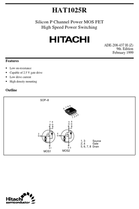
Outline
SOP–8
8 5 7 6
3 1 2 7 8 D D 5 6 D D
4
2 G
4 G
S1
S3
1, 3 Source 2, 4 Gate 5, 6, 7, 8 Drain
MOS1
MOS2
HAT1025R
Absolute Maximum Ratings (Ta = 25°C)
Item Drain to source
voltage Gate to source
voltage Drain current Drain peak current Symbol VDSS VGSS ID I D(pulse)
Note1
Ratings – 20 ± 10 – 4.5 – 36 – 4.5
Unit V V A A A W W °C °C
Body–drain diode reverse drain current I DR Channel dissipation Channel dissipation Channel temperature Storage temperature Note: Pch Pch Tch Tstg
Note2 Note3
2 3 150 – 55 to + 150
1. PW ≤ 10 µs, duty cycle ≤ 1 % 2. 1 Drive operation : When using the glass epoxy board (FR4 40 x 40 x 1.6 mm), PW≤ 10s 3. 2 Drive operation : When using the glass epoxy board (FR4 40 x 40 x 1.6 mm), PW≤ 10s
Electrical Characteristics (Ta = 25°C)
Item Symbol Min – 20 ± 10 — — – 0.5 — — 4.5 — — — — — — — — — Typ — — — — — 0.065 0.09 7 860 450 150 20 120 120 100 – 0.9 60 Max — — ± 10 – 10 – 1.5 0.095 0.15 — — — — — — — — – 1.4 — Unit V V µA µA V Ω Ω S pF pF pF ns ns ns ns V ns IF = – 4.5 A, VGS = 0 Note4 IF = – 4.5 A, VGS = 0 diF/ dt = 20 A/µs Test Conditions I D = – 10 mA, VGS = 0 I G = ± 100 µA, VDS = 0 VGS = ± 8 V, VDS = 0 VDS = – 20 V, VGS = 0 VDS = – 10 V, I D = – 1 mA I D = – 3 A, VGS = – 4 V Note4 I D = – 3 A, VGS = – 2.5 V Note4 I D...