HAT3008R/HAT3008RJ
Silicon N/P Channel Power MOS FET High Speed Power Switching
ADE-208-536B (Z) 3rd. Edition February ...
HAT3008R/HAT3008RJ
Silicon N/P Channel Power MOS FET High Speed Power Switching
ADE-208-536B (Z) 3rd. Edition February 1999 Features
For Automotive Application ( at Type Code “J “) Low on-resistance Capable of 4 V gate drive High density mounting
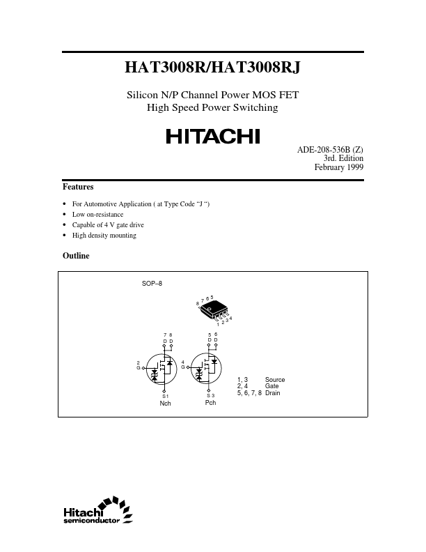
Outline
SOP–8
8 5 7 6
3 1 2 7 8 D D 5 6 D D
4
2 G
4 G
S1
S3
1, 3 Source 2, 4 Gate 5, 6, 7, 8 Drain
Nch
Pch
HAT3008R/HAT3008RJ
Absolute Maximum Ratings (Ta = 25°C)
Item Symbol Ratings Nch Drain to source
voltage Gate to source
voltage Drain current Drain peak current Body-drain diode reverse drain current Avalanche current HAT3008R HAT3008RJ Avalanche energy HAT3008R HAT3008RJ Channel dissipation Channel dissipation Channel temperature Storage temperature Note: 1. 2. 3. 4. Pch Pch Tch Tstg
Note2 Note3
Unit Pch – 60 ± 20 – 3.5 – 28 – 3.5 V V A A A
VDSS VGSS ID I D(pulse) I DR I AP Note4
Note4 Note1
60 ±20 5 40 5
— 5
— – 3.5 — 1.05 2 3 150 –55 to + 150
— A — mJ W W °C °C
EAR
— 2.14 2 3 150 – 55 to + 150
PW ≤ 10 µs, duty cycle ≤ 1 % 1 Drive operation : When using the glass epoxy board (FR4 40 x 40 x 1.6 mm), PW≤ 10s 2 Drive operation : When using the glass epoxy board (FR4 40 x 40 x 1.6 mm), PW≤ 10s Value at Tch=25°C, Rg≥50Ω
2
HAT3008R/HAT3008RJ
Electrical Characteristics (Ta = 25°C)
( N Channel ) Item Drain to source breakdown
voltage Gate to source breakdown
voltage Gate to source leak current Zero gate
voltage drain current Zero gate
voltage drain current HAT3008R Symbol Min V(BR)DSS V(BR)GSS I GSS I DSS...