HCC4007UB HCF4007UB
DUAL COMPLEMENTARY PAIR PLUS INVERTER
. . . . . .
STANDARDIZED SYMMETRICAL OUTPUT CHARACTERISTICS ...
HCC4007UB HCF4007UB
DUAL COMPLEMENTARY PAIR PLUS INVERTER
. . . . . .
STANDARDIZED SYMMETRICAL OUTPUT CHARACTERISTICS MEDIUM SPEED OPERATION tPHL, tPLH = 30ns (typ.) AT 10V QUIESCENT CURRENT SPECIFIED TO 20V FOR HCC DEVICE INPUT CURRENT OF 100nA AT 18V AND 25oC FOR HCC DEVICE 100% TESTED FOR QUIESCENT CURRENT MEETS ALL REQUIREMENTS OF JEDEC TENTATIVE STANDARD No 13A, ”STANDARD SPECIFICATIONS FOR DESCRIPTION OF B SERIES
CMOS DEVICES”
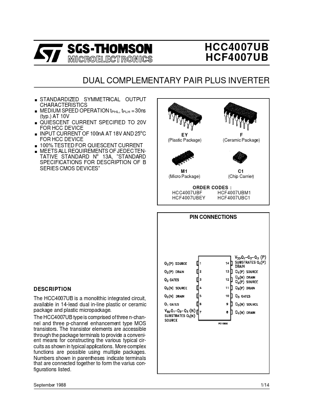
EY (Plastic Package)
F (Ceramic Package)
M1 (Micro Package)
C1 (Chip Carrier)
ORDER CODES : HCC4007UBF HCF4007UBM1 HCF4007UBEY HCF4007UBC1
PIN CONNECTIONS
DESCRIPTION The HCC4007UB is a monolithic integrated circuit, available in 14-lead dual in-line plastic or ceramic package and plastic micropackage. The HCC4007UB type is comprised of three n-channel and three p-channel enhancement type MOS transistors. The transistor elements are accessible through the package terminals to provide a convenient means for constructing the various typical circuits as shown in typical applications. More complex functions are possible using multiple packages. Numbers shown in parentheses indicate terminals that are connected together to form the varius configurations listed.
September 1988 1/14
HCC/HCF4007UB
FUNCTIONAL DIAGRAM
ABSOLUTE MAXIMUM RATING
Symbol VDD * Vi II Ptot Parameter Supply
Voltage: HCC Types HCF Types Input
Voltage DC Input Current (any one input) Total Power Dissipation (per package) Dissipation per Output Transistor for Top = Full Pack...