|
|
700V N-Channel Super Junction MOSFET
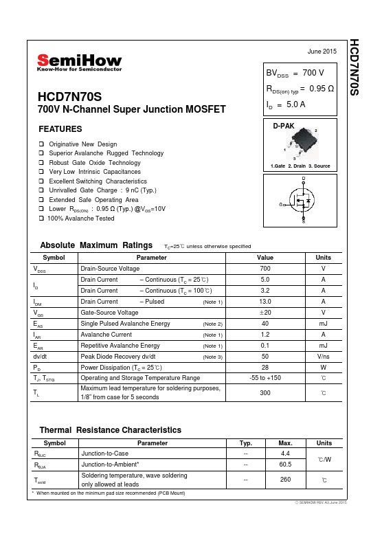
HCD7N70S HCD7N70S 700V N-Channel Super Junction MOSFET FEATURES Originative New Design Superior Avalanche Rugged Te...
| @ 2014 :: Datasheetspdf.com :: Semiconductors datasheet search & download site. (Privacy Policy & Contact) |