HD74HC240
Octal Buffers/Line Drivers/Line Receivers (with inverted 3-state outputs)
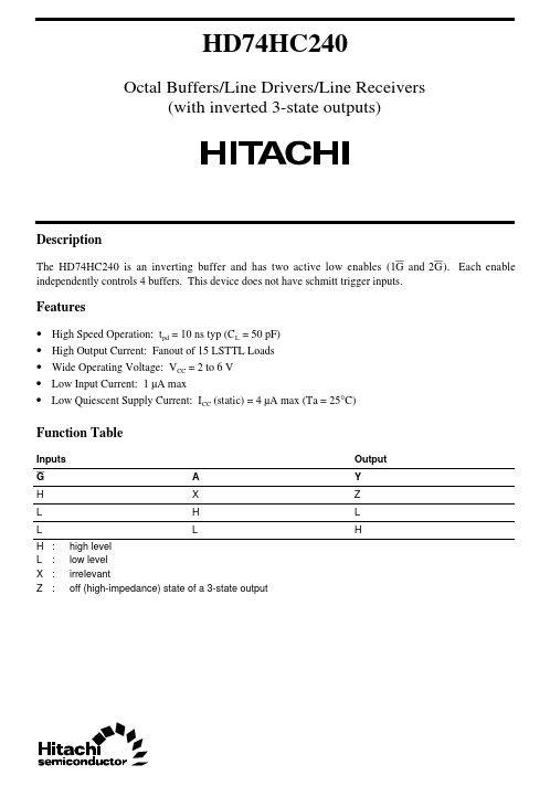
Description
The HD74HC240 is an inv...
HD74HC240
Octal Buffers/Line Drivers/Line Receivers (with inverted 3-state outputs)
Description
The HD74HC240 is an inverting buffer and has two active low enables (1G and 2G ). Each enable independently controls 4 buffers. This device does not have schmitt trigger inputs.
Features
High Speed Operation: tpd = 10 ns typ (CL = 50 pF) High Output Current: Fanout of 15 LSTTL Loads Wide Operating
Voltage: VCC = 2 to 6 V Low Input Current: 1 µA max Low Quiescent Supply Current: ICC (static) = 4 µA max (Ta = 25°C)
Function Table
Inputs G H L L H L X Z : : : : A X H L high level low level irrelevant off (high-impedance) state of a 3-state output Output Y Z L H
HD74HC240
Pin Arrangement
1G1 1A1 2Y4 1A2 2Y3 1A3 2Y2 1A4 2Y1
1 2 3 4 5 6 7 8 9
20 VCC 19 2G 18 1Y1 17 2A4 16 1Y2 15 2A3 14 1Y3 13 2A2 12 1Y4 11 2A1 (Top view)
GND 10
Absolute Maximum Ratings
Item Supply
voltage range Input
voltage Output
voltage DC current drain per pin DC current drain per VCC, GND DC input diode current DC output diode current Power dissipation per package Storage temperature Symbol VCC VIN VOUT I OUT I CC, I GND I IK I OK PT Tstg Rating –0.5 to +7.0 –0.5 to VCC + 0.5 –0.5 to VCC + 0.5 ±35 ±75 ±20 ±20 500 –65 to +150 Unit V V V mA mA mA mA mW °C
2
HD74HC240
Logic Diagram
To three other 7 inverters One of 8 inverters
VCC Input A
Y
Strobe G
3
HD74HC240
DC Characteristics
Ta = 25°C Item Input
voltage Symbol VIH Ta = –40 to +85°C Max — — — 0.5 1.35 1.8 — — — — — 0.1 0.1 0.1 0.33 0.33 ±5...