HD74HC273
Octal D-type Flip-Flops (with Clear)
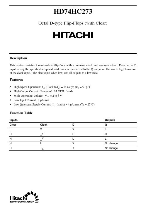
Description
This device contains 8 master-slave flip-flops with a common...
HD74HC273
Octal D-type Flip-Flops (with Clear)
Description
This device contains 8 master-slave flip-flops with a common clock and common clear. Data on the D input having the specified setup and hold times is transferred to the Q output on the low to high transition of the clock input. The clear input when low, sets all outputs to a low state.
Features
High Speed Operation: tpd (Clock to Q) = 18 ns typ (CL = 50 pF) High Output Current: Fanout of 10 LSTTL Loads Wide Operating
Voltage: VCC = 2 to 6 V Low Input Current: 1 µA max Low Quiescent Supply Current: ICC (static) = 4 µA max (Ta = 25°C)
Function Table
Inputs Clear L H H H H L Clock X D X H L X X Outputs Q L H L No change No change
HD74HC273
Pin Arrangement
Clear 1Q 1D 2D 2Q 3Q 3D 4D 4Q
1 2 3 4 5 6 7 8 9
20 VCC
Q Q
19 8Q 18 8D 17 7D 16 7Q 15 6Q 14 6D 13 5D 12 5Q 11 Clock
Clear
D CK
Clear
CK D
D Q
CK
CK
D Q
Clear
Clear
Q
Q
Clear
D CK
Clear
CK D
D Q
CK
CK
D Q
Clear
Clear
GND 10 (Top view)
2
HD74HC273
Logic Diagram
Clock 1D Clear
CK Q CK D CL Q
1Q
2D
D CL
2Q
CK
3D
D CL
Q
3Q
CK
4D
D CL CK
Q
4Q
5D
D CL
Q
5Q
CK
6D
D CL
Q
6Q
CK
7D
D CL
Q
7Q
CK
8D
D CL
Q
8Q
3
HD74HC273
DC Characteristics
Ta = 25°C Item Input
voltage Symbol VIH Ta = –40 to +85°C Max — — — 0.5 1.35 1.8 — — — — — 0.1 0.1 0.1 0.33 0.33 ±1.0 40 µA µA I OL = 4 mA I OL = 5.2 mA Vin = VCC or GND Vin = VCC or GND, Iout = 0 µA V I OH = –4 mA I OH = –5.2 mA Vin = VIH or VIL I OL = 20 µA V Vin = VIH or ...