HD74HC352
Dual 4-to-1-line Data Selectors/Multiplexers
Description
Each of these data selectors/multiplexers contains i...
HD74HC352
Dual 4-to-1-line Data Selectors/Multiplexers
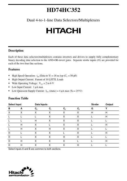
Description
Each of these data selectors/multiplexers contains inverters and drivers to supply fully complementary binary decoding data selection to the AND-OR-invert gates. Separate strobe inputs (G) are provided for each of the two four-line sections.
Features
High Speed Operation: tpd (Data to Y) = 16 ns typ (CL = 50 pF) High Output Current: Fanout of 10 LSTTL Loads Wide Operating
Voltage: VCC = 2 to 6 V Low Input Current: 1 µA max Low Quiescent Supply Current: ICC (static) = 4 µA max (Ta = 25°C)
Function Table
Select Input B X L L L L H H H H A X L L H H L L H H Data Inputs C0 X L H X X X X X X C1 X X X L H X X X X C2 X X X X X L H X X C3 X X X X X X X L H Strobe G H L L L L L L L L Output Y H H L H L H L H L
Select inputs A and B are common to both sections
HD74HC352
Pin Arrangement
Strobe 1G Select B 1C3 Data inputs 1C2 1C1 1C0 Output 1Y GND
1 2 3 4 5 6 7 8
16 15 14 13 12 11 10 9
VCC Strobe 2G Select A 2C3 2C2 2C1 2C0 Output 2Y Data inputs
(Top view)
2
HD74HC352
Logic Diagram
1G 1C0 1C1 1C2 1C3 1Y
B A
2C0 2C1 2C2 2C3 2G 2Y
3
HD74HC352
DC Characteristics
Ta = 25°C Item Input
voltage Symbol VIH Ta = –40 to +85°C Max — — — 0.5 1.35 1.8 — — — — — 0.1 0.1 0.1 0.33 0.33 ±1.0 40 µA µA I OL = 4 mA I OL = 5.2 mA Vin = VCC or GND Vin = VCC or GND, Iout = 0 µA V I OH = –4 mA I OH = –5.2 mA Vin = VIH or VIL I OL = 20 µA V Vin = VIH or VIL I OH = –20 µA V Unit V Test Conditions
VCC (V) Min Typ Max Min ...