HD74LV1GT04A
Inverter / CMOS Logic Level Shifter
REJ03D0117-0900 Rev.9.00 Mar 21, 2008
www.DataSheet4U.net
Description
...
HD74LV1GT04A
Inverter /
CMOS Logic Level Shifter
REJ03D0117-0900 Rev.9.00 Mar 21, 2008
www.DataSheet4U.net
Description
The HD74LV1GT04A has an inverter in a 5 pin package. The input protection circuitry on this device allows over
voltage tolerance on the input, allowing the device to be used as a logic–level translator from 3.0 V
CMOS Logic to 5.0 V
CMOS Logic or from 1.8 V
CMOS logic to 3.0 V
CMOS Logic while operating at the high-
voltage power supply. Low
voltage and high-speed operation is suitable for the battery powered products (e.g., notebook computers), and the low power consumption extends the battery life.
Features
The basic gate function is lined up as Renesas uni logic series. Supplied on emboss taping for high-speed automatic mounting. TTL compatible input level. Supply
voltage range : 3.0 to 5.5 V Operating temperature range : –40 to +85°C Logic-level translate function 3.0 V
CMOS logic → 5.0 V
CMOS logic (@VCC = 5.0 V) 1.8 V or 2.5 V
CMOS logic → 3.3 V
CMOS logic (@VCC = 3.3 V) All inputs VIH (Max.) = 5.5 V (@VCC = 0 V to 5.5 V) All outputs VO (Max.) = 5.5 V (@VCC = 0 V) Output current ±6 mA (@VCC = 3.0 V to 3.6 V), ±12 mA (@VCC = 4.5 V to 5.5 V) All the logical input has hysteresis
voltage for the slow transition. Ordering Information
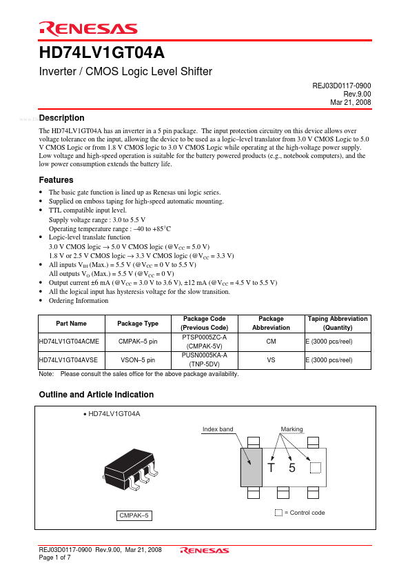
Part Name HD74LV1GT04ACME HD74LV1GT04AVSE Note: Package Type CMPAK–5 pin VSON–5 pin Package Code (Previous Code) PTSP0005ZC-A (CMPAK-5V) PUSN0005KA-A (TNP-5DV) Package Abbreviation CM VS Taping Abbreviation (Qua...