Data Sheet
HD74LV1GW16A
Dual Buffer
R04DS0032EJ0300 Rev.3.00
Jan 10, 2014
Description
The HD74LV1GW16A has dual buffe...
Data Sheet
HD74LV1GW16A
Dual Buffer
R04DS0032EJ0300 Rev.3.00
Jan 10, 2014
Description
The HD74LV1GW16A has dual buffer in a 6 pin package. Low
voltage and high-speed operation is suitable for the battery powered products (e.g., notebook computers), and the low power consumption extends the battery life.
Features
The basic gate function is lined up as Renesas uni logic series.
Supplied on emboss taping for high-speed automatic mounting.
Supply
voltage range : 1.65 to 5.5 V Operating temperature range : –40 to +85°C
All inputs VIH (Max.) = 5.5 V (@VCC = 0 V to 5.5 V) All outputs VO (Max.) = 5.5 V (@VCC = 0 V)
Output current ±6 mA (@VCC = 3.0 V to 3.6 V), ±12 mA (@VCC = 4.5 V to 5.5 V) All the logical input has hysteresis
voltage for the slow transition.
Ordering Information
Part Name
Package Type
Package Code (Previous Code)
Package Abbreviation
HD74LV1GW16ACME CMPAK-6 pin
PTSP0006JA-A (CMPAK-6V)
CM
Taping Abbreviation (Quantity)
E (3,000 pcs / Reel)
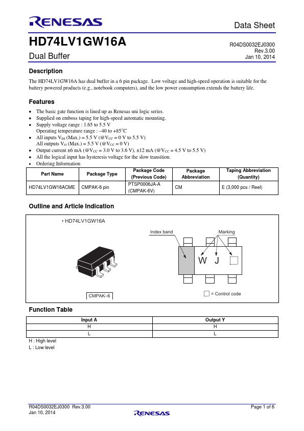
Outline and Article Indication
HD74LV1GW16A
Index band
Marking
WJ
CMPAK–6
Function Table
H : High level L : Low level
Input A H L
= Control code
Output Y H L
R04DS0032EJ0300 Rev.3.00 Jan 10, 2014
Page 1 of 6
HD74LV1GW16A
Pin Arrangement
1A 1 GND 2
2A 3
6 1Y 5 VCC 4 2Y
(Top view)
Absolute Maximum Ratings
Item
Symbol
Ratings
Unit Test Conditions
Supply
voltage range Input
voltage range *1
Output
voltage range *1, 2
Input clamp current Output clamp current Continuous output current...