HD74LV1GW58A
Configurable Multiple–Function Gate
REJ03D0082-0200 Rev.2.00 May 19, 2006
www.DataSheet4U.net
Description
...
HD74LV1GW58A
Configurable Multiple–Function Gate
REJ03D0082-0200 Rev.2.00 May 19, 2006
www.DataSheet4U.net
Description
The HD74LV1GW58A has configurable multiple–function gate in a 6 pin package. The Output state is determined by eight patterns of 3–bit input. The user can choose the logic functions AND, NAND, OR, NOR, EX–OR. Low
voltage and high speed operation is suitable for the battery powered products (e.g., notebook computers), and the low power consumption extends the battery life.
Features
The basic gate function is lined up as Renesas uni logic series. Supplied on emboss taping for high speed automatic mounting. Supply
voltage range : 1.65 to 5.5 V Operating temperature range : –40 to +85°C All inputs VIH (Max.) = 5.5 V (@VCC = 0 V to 5.5 V) All outputs VO (Max.) = 5.5 V (@VCC = 0 V) Output current ±6 mA (@VCC = 3.0 V to 3.6 V), ±12 mA (@VCC = 4.5 V to 5.5 V) All the logical input has hysteresis
voltage for the slow transition. Ordering Information
Part Name Package Type CMPAK-6 pin Package Code (Previous Code) PTSP0006-JA-A (CMPAK-6V) Package Abbreviation CM Taping Abbreviation (Quantity) E (3,000 pcs / Reel)
HD74LV1GW58ACME
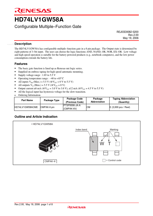
Outline and Article Indication
HD74LV1GW58A
Index band Marking
W T
CMPAK–6
= Control code
Rev.2.00, May 19, 2006 page 1 of 8
HD74LV1GW58A
Function Table
IN2 L L L L H H H H H : High level L : Low level Inputs IN1 L L H H L L H H IN0 L H L H L H L H Output Y L H L H H H L L
Pin Arrangement
IN1
1
6
IN2
GND
2
...