www.DataSheet4U.com
HD74LV2G74A
Single D–type Flip Flops with Preset and Clear
REJ03D0097–0500 (Previous: ADE-205-346D)...
www.DataSheet4U.com
HD74LV2G74A
Single D–type Flip Flops with Preset and Clear
REJ03D0097–0500 (Previous: ADE-205-346D) Rev.5.00 Apr 07, 2006
Description
The HD74LV2G74A has independent data, preset, clear, and clock inputs Q and Q outputs in an 8 pin package. The input data is transferred to the output at the rising edge of clock pulse CLK. Low
voltage and high-speed operation is suitable for the battery powered products (e.g., notebook computers), and the low power consumption extends the battery life.
Features
The basic gate function is lined up as Renesas uni logic series. Supplied on emboss taping for high-speed automatic mounting. Electrical characteristics equivalent to the HD74LV74A Supply
voltage range : 1.65 to 5.5 V Operating temperature range : –40 to +85°C All inputs VIH (Max.) = 5.5 V (@VCC = 0 V to 5.5 V) All outputs VO (Max.) = 5.5 V (@VCC = 0 V) Output current ±6 mA (@VCC = 3.0 V to 3.6 V), ±12 mA (@VCC = 4.5 V to 5.5 V) All the logical input has hysteresis
voltage for the slow transition. Ordering Information
Part Name Package Type Package Code (Previous code) PVSP0008KA-A (TTP-8DBV) US Package Abbreviation Taping Abbreviation (Quantity) E (3,000 pcs / Reel)
HD74LV2G74AUSE SSOP-8 pin
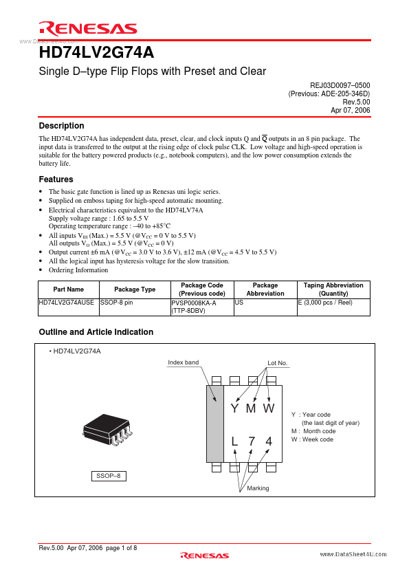
Outline and Article Indication
HD74LV2G74A
Index band Lot No.
Y M W L 7 4
SSOP–8 Marking
Y : Year code (the last digit of year) M : Month code W : Week code
Rev.5.00 Apr 07, 2006 page 1 of 8
HD74LV2G74A
www.DataSheet4U.com Function Table
Inputs PRE L H ...