HI-8588
January 2001
DESCRIPTION
The HI-8588 is an ARINC 429 bus interface receiver and is available in a SO 8 pin pack...
HI-8588
January 2001
DESCRIPTION
The HI-8588 is an ARINC 429 bus interface receiver and is available in a SO 8 pin package. The technology is analog/digital
CMOS. The circuitry requires only a 5 volt supply. The ARINC bus can be connected directly to the chip. The typical 10 volt differential signal is translated and input to a window comparator and latch. The comparator levels are just below the standard 6.5 volt minimum ARINC data threshold and just above the standard 2.5 volt maximum ARINC null threshold. The TESTA and TESTB inputs bypass the analog for testing purposes. Also if TESTA and TESTB are both taken high, the analog powers down and the digital outputs tri-state allowing wire-or possibilities. Please refer to the HI-8588-10 for applications where an external resistance in series with the ARINC inputs is required for lightning protection or when the digital outputs need to be a logic zero rather than open circuit when TESTA and TESTB are both high.
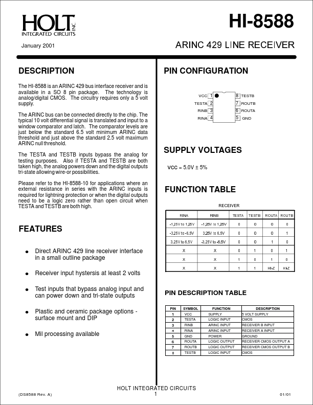
PIN CONFIGURATION
VCC 1 TESTA 2 RINB 3 RINA 4
8 TESTB 7 ROUTB 6 ROUTA 5 GND
SUPPLY
VOLTAGES
vcc = 5.0V ± 5%
FUNCTION TABLE
FEATURES
! ! ! ! !
Direct ARINC 429 line receiver interface in a small outline package Receiver input hystersis at least 2 volts Test inputs that bypass analog input and can power down and tri-state outputs Plastic and ceramic package options surface mount and DIP Mil processing available
PIN DESCRIPTION TABLE
PIN SYMBOL VCC TESTA RINB RINA GND ROUTA ROUTB TESTB FUNCTION SUPPLY LOGIC INPUT A...