AMPLIFIERS - LOW NOISE - CHIP
v11.0617
1 Typical Applications The HMC463 is ideal for: • Telecom Infrastructure • Micro...
AMPLIFIERS - LOW NOISE - CHIP
v11.0617
1 Typical Applications The HMC463 is ideal for: Telecom Infrastructure Microwave Radio & VSAT Military & Space Test Instrumentation Fiber Optics Functional Diagram
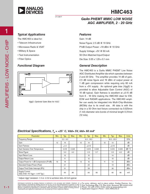
Vgg2: Optional Gate Bias for AGC
HMC463
GaAs PHEMT MMIC LOW NOISE AGC AMPLIFIER, 2 - 20 GHz
Features
Gain: 14 dB Noise Figure: 2.5 dB @ 10 GHz P1dB Output Power: +19 dBm @ 10 GHz Supply
Voltage: +5V @ 60 mA 50 Ohm Matched Input/Output Die Size: 3.05 x 1.29 x 0.1 mm
General Description
The HMC463 is a GaAs MMIC PHEMT Low Noise AGC Distributed Amplifier die which operates between 2 and 20 GHz. The amplifier provides 14 dB of gain, 2.5 dB noise figure and 19 dBm of output power at 1 dB gain compression while requiring only 60 mA from a +5V supply. An optional gate bias (Vgg2) is provided to allow Adjustable Gain Control (AGC) of 10 dB typical. Gain flatness is excellent at ±0.15 dB from 6 - 18 GHz making the HMC463 ideal for EW, ECM and RADAR applications. The HMC463 amplifier can easily be integrated into Multi-Chip-Modules (MCMs) due to its small size. All data is with the chip in a 50 Ohm test fixture connected via 0.025mm (1 mil) diameter wire bonds of minimal length 0.31mm (12 mils).
1-1
Electrical Specifications, TA = +25° C, Vdd= 5V, Idd= 60 mA*
Parameter Frequency Range Gain Gain Flatness Gain Variation Over Temperature Noise Figure Input Return Loss Output Return Loss Output Power for 1 dB Compression (P1dB) Saturated Output Power (Psat) Output Third Order...