LOW NOISE AMPLIFIERS - SMT
8
8 - 126
HMC491LP3 / 491LP3E
v03.1206
GaAs MMIC LOW NOISE AMPLIFIER w/ BYPASS MODE, 3.4 ...
LOW NOISE
AMPLIFIERS - SMT
8
8 - 126
HMC491LP3 / 491LP3E
v03.1206
GaAs MMIC LOW NOISE AMPLIFIER w/ BYPASS MODE, 3.4 - 3.8 GHz
Typical Applications
Features
The HMC491LP3 / HMC491LP3E is ideal for:
Gain: 16 dB
Wireless Local Loop (WLL)
Noise Figure: 2 dB
Fixed Wireless Access
Single Supply: +3V @ 9 mA
Microwave & VSAT Radios
Integrated Bypass Mode
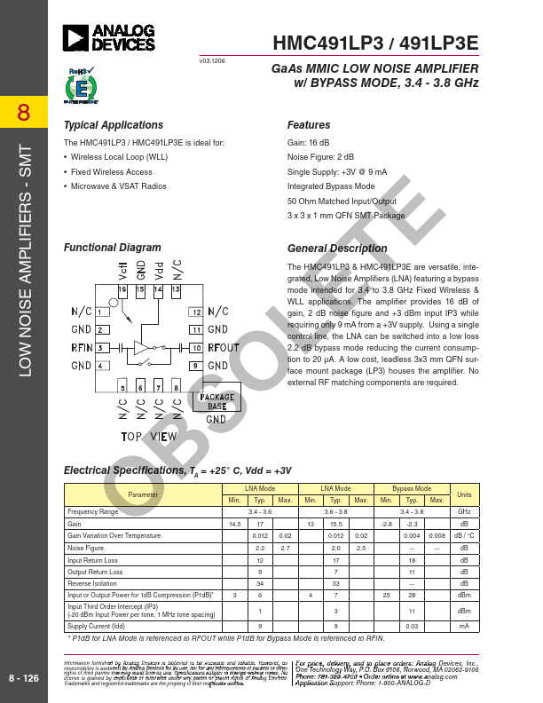
LETE Functional Diagram
50 Ohm Matched Input/Output 3 x 3 x 1 mm QFN SMT Package
General Description
The HMC491LP3 & HMC491LP3E are versatile, integrated, Low Noise
Amplifiers (LNA) featuring a bypass mode intended for 3.4 to 3.8 GHz Fixed Wireless & WLL applications. The amplifier provides 16 dB of gain, 2 dB noise figure and +3 dBm input IP3 while requiring only 9 mA from a +3V supply. Using a single control line, the LNA can be switched into a low loss 2.2 dB bypass mode reducing the current consumption to 20 μA. A low cost, leadless 3x3 mm QFN surface mount package (LP3) houses the amplifier. No external RF matching components are required.
SO Electrical Specifications, TA = +25° C, Vdd = +3V
B Parameter O Frequency Range
LNA Mode Min. Typ. Max.
3.4 - 3.6
LNA Mode Min. Typ. Max.
3.6 - 3.8
Bypass Mode Min. Typ. Max.
3.4 - 3.8
Units GHz
Gain
14.5 17
13 15.5
-2.8 -2.3
dB
Gain Variation Over Temperature
0.012 0.02
0.012 0.02
0.004 0.008 dB / °C
Noise Figure
2.2
2.7
2.0
2.5
--
--
dB
Input Return Loss
12
17
18
dB
Output Return Loss
9
7
11
dB
Reverse Isolation
34
33
--
dB
Inpu...