HMC530LP5 / 530LP5E
v07.0411
MMIC VCO w/ HALF FREQUENCY OUTPUT & DIVIDE-BY-4, 9.5 - 10.8 GHz
Typical Applications
Low n...
HMC530LP5 / 530LP5E
v07.0411
MMIC VCO w/ HALF FREQUENCY OUTPUT & DIVIDE-BY-4, 9.5 - 10.8 GHz
Typical Applications
Low noise MMIC VCO w/Half Frequency, Divide-by-4 Outputs for: Point to Point/Multipoint Radio Test Equipment & Industrial Controls SATCOM Military End-Use
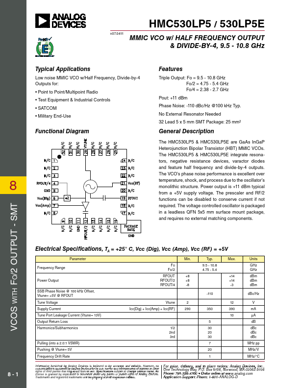
Functional Diagram
Features
Triple Output: Fo = 9.5 - 10.8 GHz Fo/2 = 4.75 - 5.4 GHz Fo/4 = 2.38 - 2.7 GHz
Pout: +11 dBm Phase Noise: -110 dBc/Hz @100 kHz Typ. No External Resonator Needed 32 Lead 5 x 5 mm SMT Package: 25 mm²
General Description
The HMC530LP5 & HMC530LP5E are GaAs InGaP
Heterojunction Bipolar Transistor (HBT) MMIC VCOs.
The HMC530LP5 & HMC530LP5E integrate resona-
tors, negative resistance devices, varactor diodes
and feature half frequency and divide-by-4 outputs.
The VCO’s phase noise performance is excellent over
8
temperature, shock, and process due to the oscillator’s monolithic structure. Power output is +11 dBm typical
from a +5V supply
voltage. The prescaler and RF/2
functions can be disabled to conserve current if not
required. The
voltage controlled oscillator is packaged
in a leadless QFN 5x5 mm surface mount package,
and requires no external matching components.
VCOS with Fo/2 OUTPUT - SMT
8-1
Electrical Specifications, TA = +25° C, Vcc (Dig), Vcc (Amp), Vcc (RF) = +5V
Parameter Frequency Range
Power Output
SSB Phase Noise @ 100 kHz Offset, Vtune= +5V @ RFOUT Tune
Voltage Supply Current Tune Port Leakage Current (Vtune= 13V) Output Return Loss Harmonics/Sub...