DRIVER & GAIN BLOCK AMPLIFIERS - CHIP
v04.1108
Typical Applications
2
The HMC562 wideband driver is ideal for:
• Mi...
DRIVER & GAIN BLOCK
AMPLIFIERS - CHIP
v04.1108
Typical Applications
2
The HMC562 wideband driver is ideal for:
Military & Space
Test Instrumentation
Fiber Optics
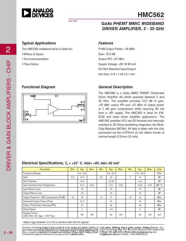
Functional Diagram
HMC562
GaAs PHEMT MMIC WIDEBAND DRIVER AMPLIFIER, 2 - 35 GHz
Features
P1dB Output Power: +18 dBm Gain: 12.5 dB Output IP3: +27 dBm Supply
Voltage: +8V @ 80 mA 50 Ohm Matched Input/Output Die Size: 3.12 x 1.42 x 0.1 mm
General Description
The HMC562 is a GaAs MMIC PHEMT Distributed Driver Amplifier die which operates between 2 and 35 GHz. The amplifier provides 12.5 dB of gain, +19 dBm output IP3 and +12 dBm of output power at 1 dB gain compression while requiring 80 mA from a +8V supply. The HMC562 is ideal for EW, ECM and radar driver amplifier applications. The HMC562 amplifier I/O’s are DC blocked and internally matched to 50 Ohms facilitating integration into MultiChip-Modules (MCMs). All data is taken with the chip connected via two 0.075mm (3 mil) ribbon bonds of minimal length 0.31mm (12 mils).
2 - 34
Electrical Specifications, TA = +25° C, Vdd= +8V, Idd= 80 mA*
Parameter Frequency Range Gain Gain Flatness Gain Variation Over Temperature Input Return Loss Output Return Loss Output Power for 1 dB Compression (P1dB) Saturated Output Power (Psat) Output Third Order Intercept (IP3) Noise Figure Supply Current (Idd) (Vdd= 8V, Vgg = -0.8V Typ.)
Min. Typ. Max.
2.0 - 15.0
9.5
12.5
±0.4
0.01 0.02
14
16
15
18
21.5
27
3
80
100
Min.
Typ. Max.
15.0 - 27.0
8.5
12
±0....