LOW NOISE AMPLIFIERS - SMT
HMC605LP3 / 605LP3E
v04.1013
GaAs PHEMT MMIC LOW NOISE
AMPLIFIER w/ BYPASS MODE, 2.3 - 2....
LOW NOISE
AMPLIFIERS - SMT
HMC605LP3 / 605LP3E
v04.1013
GaAs PHEMT MMIC LOW NOISE
AMPLIFIER w/ BYPASS MODE, 2.3 - 2.7 GHz
Typical Applications
Features
The HMC605LP3 / HMC605LP3E is ideal for:
Noise Figure: 1.1 dB
Wireless Infrastructure
Output IP3: +31 dBm
Customer Premise Equipment
Gain: 20 dB
Fixed Wireless
Low Loss & Failsafe Bypass Path
WiMAX & WiBro Tower Mounted
Amplifiers
Single Supply: +3V or +5V 50 Ohm Matched Output/Input
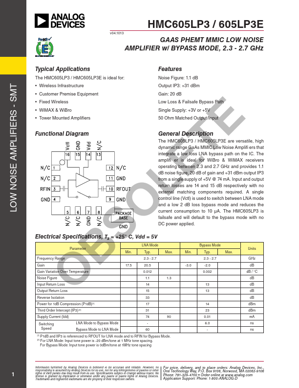
OLETE Functional Diagram
General Description
The HMC605LP3 / HMC605LP3E are versatile, high dynamic range GaAs MMIC Low Noise Amplifi ers that integrate a low loss LNA bypass path on the IC. The amplifi er is ideal for WiBro & WiMAX receivers operating between 2.3 and 2.7 GHz and provides 1.1 dB noise figure, 20 dB of gain and +31 dBm output IP3 from a single supply of +5V @ 74 mA. Input and output return losses are 14 and 15 dB respectively with no external matching components required. A single control line (Vctl) is used to switch between LNA mode and a low 2 dB loss bypass mode and reduces the current consumption to 10 μA. The HMC605LP3 is failsafe and will default to the bypass mode with no DC power applied.
Electrical Specifications, TA = +25° C, Vdd = 5V
S Parameter
LNA Mode
Min.
Typ.
Max.
Frequency Range
2.3 - 2.7
B Gain
17.5
20.5
Gain Variation Over Temperature
0.012
Noise Figure
1.1
1.3
O Input Return Loss
14
Bypass Mode
Min.
Typ.
Max.
2.3 - 2.7
-3.0
-2.0
0.002
13
Units
GHz dB dB / ...