www.DataSheet4U.com
DATASHEET
LOW SKEW 1 TO 4 CLOCK BUFFER Description
The ICS524 is a low skew, single input to four ...
www.DataSheet4U.com
DATASHEET
LOW SKEW 1 TO 4 CLOCK BUFFER Description
The ICS524 is a low skew, single input to four output, clock buffer. Part of ICS’ ClockBlocksTM family, this is our lowest skew, small clock buffer. See the ICS552-02 for a 1 to 8 low skew buffer. For more than eight outputs, see the MK74CBxxx BuffaloTM series of clock drivers. ICS makes many non-PLL and PLL based low skew output devices as well as Zero Delay Buffers to synchronize clocks. Contact us for all of your clocking needs.
ICS524 Features
Extremely low skew outputs (50 ps maximum) Packaged in 8-pin SOIC Available in Pb (lead) free package Low power
CMOS technology Operating
voltages of 2.5 V to 5 V Output Enable pin tri-states outputs 5 V tolerant input clock Industrial temperature range
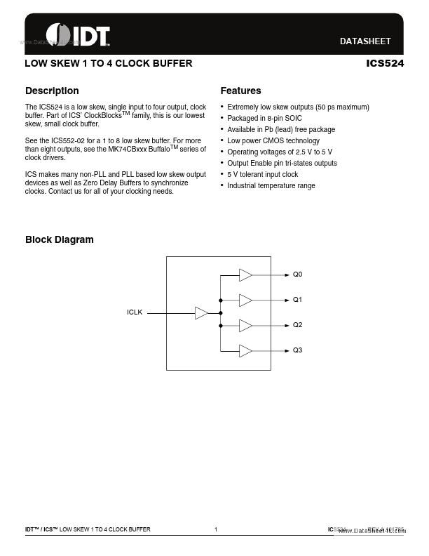
Block Diagram
Q0 Q1 ICLK Q2 Q3
IDT™ / ICS™ LOW SKEW 1 TO 4 CLOCK BUFFER
1
ICS524
REV A 101705
ICS524 LOW SKEW 1 TO 4 CLOCK BUFFER
www.DataSheet4U.com
FAN OUT BUFFER
Pin Assignment
ICLK Q0 Q1 NC 1 2 3 4 8 7 6 5 8-pin SOIC GND Q3 Q2 VDD
Pin Descriptions
Pin Pin Number Name
1 2 3 4 5 6 7 8 ICLK Q0 Q1 NC VDD Q2 Q3 GND
Pin Type
Input Output Output Power Output Output Power Clock input, 5V tolerant input. Clock output 0. Clock output 1.
Pin Description
Do not connect this pin to anything. Connect to +2.5 V, +3.3 V or +5.0 V. Clock Output 2. Clock Output 3. Connect to ground.
External Components
A minimum number of external components are required for proper operation. A decoupling capaci...