PCI-EXPRESS GEN1 CLOCK SOURCE
DATASHEET
ICS557-01
Description
The ICS557-01 is a clock chip designed for use in PCI-Ex...
PCI-EXPRESS GEN1 CLOCK SOURCE
DATASHEET
ICS557-01
Description
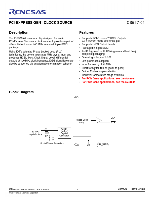
The ICS557-01 is a clock chip designed for use in PCI-Express Cards as a clock source. It provides a pair of differential outputs at 100 MHz in a small 8-pin SOIC package.
Using IDT’s patented Phase-Locked Loop (PLL) techniques, the device takes a 25 MHz crystal input and produces HCSL (Host Clock Signal Level) differential outputs at 100 MHz clock frequency. LVDS signal levels can also be supported via an alternative termination scheme.
Features
Supports PCI-ExpressTM HCSL Outputs
0.7 V current mode differential pair
Supports LVDS Output Levels Packaged in 8-pin SOIC RoHS 5 (green) or RoHS 6 (green and lead free)
compliant packaging
Operating
voltage of 3.3 V Low power consumption Input frequency of 25 MHz Short term jitter 100 ps (peak-to-peak) Output Enable via pin selection Industrial temperature range available For PCIe Gen2 applications, see the 5V41064 For PCIe Gen3 applications, see the 5V41234
Block Diagram
VDD
X1 25 MHz crystal /clock
X2
Clock Buffer/ Crystal Oscillator
Phase Lock Loop
Crystal Tuning
Capacitors
GND
OE
CLK CLK
RR(IREF)
IDT® PCI-EXPRESS GEN1 CLOCK SOURCE
1
ICS557-01 REV P 072512
ICS557-01 PCI-EXPRESS GEN1 CLOCK SOURCE
Pin Assignment
OE
1
X1
2
X2
3
GND 4
8 VDD 7 CLK 6 CLK 5 IREF
8 Pin (150 mil) SOIC
PCIE
Pin Descriptions
Pin Number
1
Pin Name
OE
2
X1
3
X2
4
GND
5
IREF
6
CLK
7
CLK
8
VDD
Pin Type
Pin Description
Input Output...