ICS650-40
ETHERNET SWITCH CLOCK SOURCE
Description
The ICS650-40 is a clock chip designed for use in Ethernet Switch app...
ICS650-40
ETHERNET SWITCH CLOCK SOURCE
Description
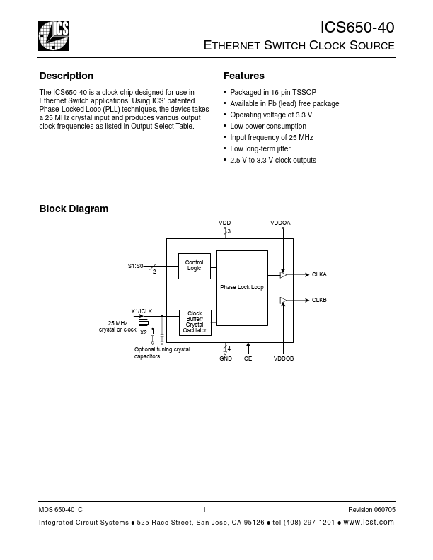
The ICS650-40 is a clock chip designed for use in Ethernet Switch applications. Using ICS’ patented Phase-Locked Loop (PLL) techniques, the device takes a 25 MHz crystal input and produces various output clock frequencies as listed in Output Select Table.
Features
Packaged in 16-pin TSSOP Available in Pb (lead) free package Operating
voltage of 3.3 V Low power consumption Input frequency of 25 MHz Low long-term jitter 2.5 V to 3.3 V clock outputs
Block Diagram
VDD 3 VDDOA
S1:S0
2
Control Logic CLKA Phase Lock Loop CLKB
X1/ICLK 25 MHz crystal or clock X2
Clock Buffer/ Crystal Oscillator 4 GND OE VDDOB
Optional tuning crystal
capacitors
MDS 650-40 C I n t e gra te d C i r c u i t S y s t e m s
●
1
525 Race Stre et, San Jo se, CA 9 5126
●
Revision 060705 te l (40 8) 2 97-12 01
●
w w w. i c st . c o m
ICS650-40 ETHERNET SWITCH CLOCK SOURCE
Pin Assignment
X1/ICLK VDD GND VDDOA CLKA CLKB VDDOB GND 1 2 3 4 5 6 7 8 16 15 14 13 12 11 10 9 X2 GND OE GND VDD VDD S1 S0
Output Select Table (MHz)
S1 0 0 1 1 S0 0 1 0 1 CLKA (MHz) 127 133 157 189 CLKB (MHz) 127 133 157 189
16-pin (173 mil) TSSOP
Pin Descriptions
Pin Number
1 2 3 4 5 6 7 8 9 10 11 12 13 14 15 16
Pin Name
X1/ICLK VDD GND VDDOA CLKA CLKB VDDOB GND S0 S1 VDD VDD GND OE GND X2
Pin Type
Input Power Power Power Connect to +3.3 V. Connect to ground.
Pin Description
Crystal or clock input. Connect to a 25 MHz crystal or single ended clock.
Connect t...