LOW SKEW 1 TO 4 CLOCK BUFFER
DATASHEET
ICS651
Description
The ICS651 is a low skew, single input to four output, clock...
LOW SKEW 1 TO 4 CLOCK BUFFER
DATASHEET
ICS651
Description
The ICS651 is a low skew, single input to four output, clock buffer. Part of IDT’s ClockBlocksTM family, this is a low skew, small clock buffer.
IDT makes many non-PLL and PLL based low skew output devices as well as Zero Delay Buffers to synchronize clocks. Contact us for all of your clocking needs.
Features
Low skew outputs (250 ps) Packaged in 8-pin SOIC RoHS 6 compliant package Low power
CMOS technology Operating
Voltages of 1.5 V to 2.5 V Output Enable pin tri-states outputs 3.3 V tolerant input clock Industrial or commercial temperature ranges
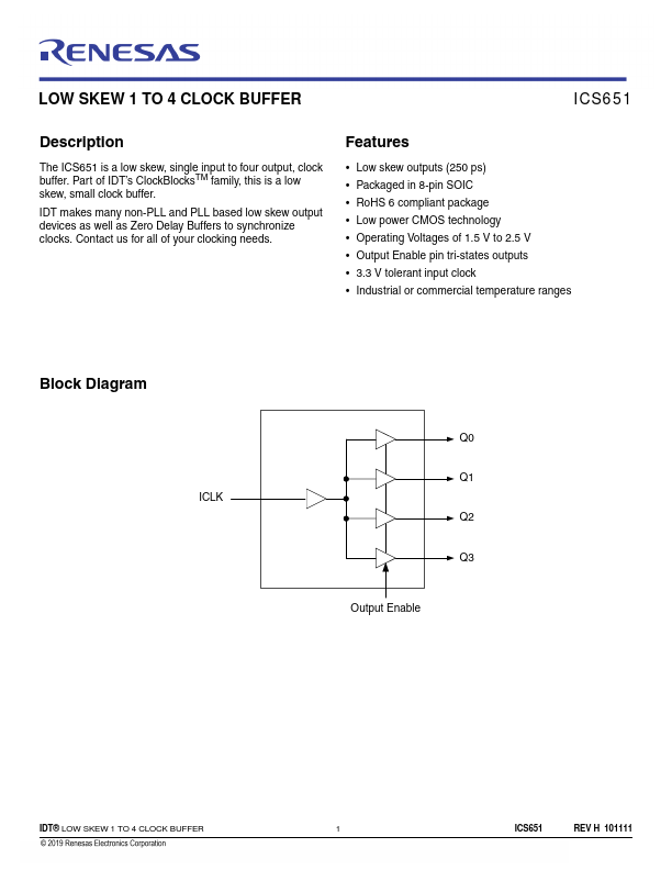
Block Diagram
ICLK
Q0 Q1 Q2 Q3
Output Enable
IDT® LOW SKEW 1 TO 4 CLOCK BUFFER
1
ICS651
REV H 101111
ICS651 LOW SKEW 1 TO 4 CLOCK BUFFER
Pin Assignment
ICLK
Q1 Q2 Q3
1 2 3 4
8 OE 7 VDD 6 GND 5 Q4
FAN OUT BUFFER
Pin Descriptions
Pin Number
1 2 3 4 5 6 7 8
Pin Name
ICLK Q1 Q2 Q3 Q4 GND VDD OE
Pin Type
Input Output Output Output Output Power Power Input
Pin Description
Clock Input. 3.3 V tolerant input. Clock Output 1. Clock Output 2. Clock Output 3. Clock Output 4. Connect to ground. Connect to +1.5 V or +2.5 V. Output Enable. Tri-states outputs when low. Connect to VDD for normal operation.
External Components
A minimum number of external components are required for proper operation. A decoupling capacitor of 0.01 μF should be connected between VDD on pin 7 and GND on pin 6, as close to the device as possible. A 33 Ω series terminating res...