Integrated Circuit Systems, Inc.
ICS8312I
LOW SKEW, 1-TO-12 LVCMOS / LVTTL FANOUT BUFFER
FEATURES
• 12 LVCMOS / LVTTL o...
Integrated Circuit Systems, Inc.
ICS8312I
LOW SKEW, 1-TO-12 LV
CMOS / LVTTL FANOUT BUFFER
FEATURES
12 LV
CMOS / LVTTL outputs LV
CMOS / LVTTL clock input Maximum output frequency: 250MHz Output skew: 160ps (maximum) Operating supply modes: Core/Output 3.3V/3.3V 2.5V/2.5V 1.8V/1.8V 3.3V/2.5V 3.3V/1.8V 2.5V/1.8V -40°C to 85°C ambient operating temperature
GENERAL DESCRIPTION
The ICS8312I is a low skew, 1-to-12 LV
CMOS / LVTTL Fanout Buffer and a member of the HiPerClockS™ HiPerClockS™family of High Performance Clock Solutions from ICS. The ICS8312I single ended clock input accepts LV
CMOS or LVTTL input levels. The low impedance LV
CMOS outputs are designed to drive 50Ω series or parallel terminated transmission lines. The effective fanout can be increased from 12 to 24 by utilizing the ability of the outputs to drive two series terminated lines. www.DataSheet4U.com
ICS
The ICS8312I is characterized at full 3.3V, 2.5V, and 1.8V, or mixed 3.3V core/2.5V, 3.3V core/1.8V and 2.5V core/1.8V output operating supply modes. Guaranteed output and part-topart skew characteristics along with the 1.8V output capabilities makes the ICS8312I ideal for high performance, single ended applications that also require a limited output
voltage.
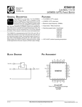
BLOCK DIAGRAM
PIN ASSIGNMENT
GND GND VDDO VDDO Q0 Q1 Q2 Q3
CLK_EN
nD Q LE 12 GND VDD Q0:Q11 CLK_EN CLK GND OE VDD GND 1 2 3 4 5 6 7 8
32 31 30 29 28 27 26 25 24 23 22 Q4 VDDO Q5 GND Q6 VDDO Q7 GND
CLK
ICS8312I
21 20 19 18 17
OE
9 10 11 1...