Differential Clock/Data Multiplexer
ICS831724I
DATA SHEET
General Description
The ICS831724I is a high-performance, di...
Differential Clock/Data Multiplexer
ICS831724I
DATA SHEET
General Description
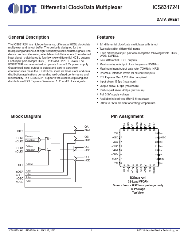
The ICS831724I is a high-performance, differential HCSL clock/data multiplexer and fanout buffer. The device is designed for the multiplexing and fanout of high-frequency clock and data signals. The device has two differential, selectable clock/data inputs. The selected input signal is distributed to four low-skew differential HCSL outputs. Each input pair accepts HCSL, LVDS and LVPECL levels. The ICS831724I is characterized to operate from a 3.3V power supply. Guaranteed input, output-to-output and part-to-part skew characteristics make the ICS831724I ideal for those clock and data distribution applications demanding well-defined performance and repeatability. The ICS831724I supports the clock multiplexing and distribution of PCI Express Generation 1, 2, and 3 clock signals.
Features
2:1 differential clock/data multiplexer with fanout Two selectable, differential inputs Each differential input pair can accept the following levels: HCSL,
LVDS, LVPECL.
Four differential HCSL outputs Maximum input/output clock frequency: 350MHz Maximum input/output data rate: 700Mb/s (NRZ) LV
CMOS interface levels for all control inputs PCI Express Gen 1,2,3 jitter compliant Input skew: 165ps (maximum) Output skew: 175ps (maximum) Part-to-part skew: 450ps (maximum) Full 3.3V supply
voltage Available in lead-free (RoHS 6) package -40°C to 85°C ambient operating temperature
Block Diagram
...