Integrated Circuit Systems, Inc.
ICS83940D
LOW SKEW, 1-TO-18 LVPECL-TO-LVCMOS / LVTTL FANOUT BUFFER
FEATURES
• 18 LVCMO...
Integrated Circuit Systems, Inc.
ICS83940D
LOW SKEW, 1-TO-18 LVPECL-TO-LV
CMOS / LVTTL FANOUT BUFFER
FEATURES
18 LV
CMOS/LVTTL outputs Selectable LV
CMOS_CLK or LVPECL clock inputs PCLK, nPCLK supports the following input types: LVPECL, CML, SSTL LV
CMOS_CLK accepts the following input levels: LV
CMOS or LVTTL Maximum output frequency: 250MHz Output skew: 150ps (maximum) Part to part skew: 750ps (maximum) Additive phase jitter, RMS: < 0.03ps (typical) Full 3.3V and 2.5V or mixed 3.3V core, 2.5V output supply modes 0°C to 70°C ambient operating temperature Lead-Free package available Pin compatible with the MPC940L
GENERAL DESCRIPTION
The ICS83940D is a low skew, 1-to-18 LVPECLto-LV
CMOS/LVTTL Fanout Buffer and a member HiPerClockS™ of the HiPerClockS™ family of High Performance Clock Solutions from ICS. The ICS83940D has two selectable clock inputs. The PCLK, nPCLK pair can accept LVPECL, CML, or SSTL input levels. The LV
CMOS_CLK can accept LV
CMOS or LVTTL input levels. The low impedance LV
CMOS/LVTTL outputs are designed to drive 50Ω series or parallel terminated transmission lines. www.DataSheet4U.com
ICS
The ICS83940D is characterized at full 3.3V and 2.5V or mixed 3.3V core, 2.5V output operating supply modes. Guaranteed output and part-to-part skew characteristics make the ICS83940D ideal for those clock distribution applications demanding well defined performance and repeatability.
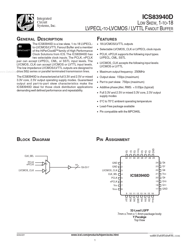
BLOCK DIAGRAM
PIN ASSIGNMENT
GND VDDO Q0 Q1 Q2 Q3 Q4 Q5
CLK_SEL P...