Integrated Circuit Systems, Inc.
ICS839893I
LOW SKEW, 1-TO-13 LVCMOS/LVTTL BUFFER DIVIDER
FEATURES
• 13 LVCMOS/LVTTL ou...
Integrated Circuit Systems, Inc.
ICS839893I
LOW SKEW, 1-TO-13 LV
CMOS/LVTTL BUFFER DIVIDER
FEATURES
13 LV
CMOS/LVTTL outputs: 3 banks (6, 6, 1 outputs per bank respectively) Selectable CLK0 or CLK1 LV
CMOS/LVTTL clock inputs CLK0, CLK1 supports the following input types: LV
CMOS, LVTTL Maximum output frequency: 250MHz Output skew: 40ps (maximum), within bank Full 3.3V or 2.5V operating supply -40°C to 85°C ambient operating temperature Available in both, Standard and RoHS/Lead-Free compliant packages
GENERAL DESCRIPTION
The ICS839893I is a high-performance one to thirteen LV
CMOS/LVTTL buffer/divider and is HiPerClockS™ a member of the HiPerClockS™ family of High Performance Clock Solutions from ICS. The device has two selectable LV
CMOS/LVTTL clock inputs and it generates 13 new LV
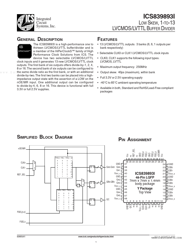
CMOS/LVTTL clock outputs. The first bank of six outputs offers divide-by-1, 2, 4, 8 or 16. The second bank of six outputs can be configured to as the first bank, or with an additional w w w . D a t the a S same h e e divide t 4 U . ratio c o m divide-by-two. The first two banks can be placed into a highimpedance output state with the assertion of a LOW on the nOE/MR input. One additional output can be configured to divide-by-4, 6, 8 or 16. This device is functional with full 3.3V or full 2.5V supplies.
IC S
SIMPLIFIED BLOCK DIAGRAM
nOE/MR
PIN ASSIGNMENT
V DD nc REF_SEL nc GND FSEL0 FSEL1 GND FSEL2 FSEL3 nOE/MR V DD
FSEL0 FSEL0 FSEL1 FSEL1 FSEL2 FSEL2QAQA 0 0 0 ÷1
0
0 0 1 1 0 0 1 1...