www.DataSheet4U.com
PRELIMINARY
Integrated Circuit Systems, Inc.
ICS844003I
FEMTOCLOCKS™CRYSTAL-TO-LVDS FREQUENCY SY...
www.DataSheet4U.com
PRELIMINARY
Integrated Circuit Systems, Inc.
ICS844003I
FEMTOCLOCKS™CRYSTAL-TO-LVDS FREQUENCY SYNTHESIZER
FEATURES
Three LVDS outputs on two banks, A Bank with one LVDS pair and B Bank with 2 LVDS output pairs Using a 31.25MHz or 26.041666MHz crystal, the two output banks can be independently set for 625MHz, 312.5MHz, 156.25MHz or 125MHz Selectable crystal oscillator interface or LV
CMOS/LVTTL single-ended input VCO range: 560MHz to 700MHz RMS phase jitter @ 156.25MHz (1.875MHz - 20MHz): 0.63ps (typical) 3.3V output supply mode -40°C to 85°C ambient operating temperature Available in both standard and lead-free RoHS-compliant packages
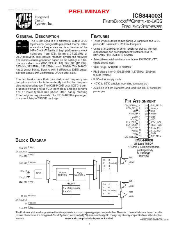
GENERAL DESCRIPTION
The ICS844003I is a 3 differential output LVDS Synthesizer designed to generate Ethernet referHiPerClockS™ ence clock frequencies and is a member of the HiPerClocks™ family of high performance clock solutions from ICS. Using a 31.25MHz or 26.041666MHz, 18pF parallel resonant crystal, the following frequencies can be generated based on the settings of 4 frequency select pins (DIV_SEL[A1:A0], DIV_SEL[B1:B0]): 625MHz, 312.5MHz, 156.25MHz, and 125MHz. The 844003I has 2 output banks, Bank A with 1 differential LVDS output pair and Bank B with 2 differential LVDS output pairs.
IC S
The two banks have their own dedicated frequency select pins and can be independently set for the frequencies mentioned above. The ICS844003I uses ICS’ 3rd generation low phase noise VCO technology and can achiev...