CRYSTAL-TO-LVDS FREQUENCY SYNTHESIZER W/INTEGRATED FANOUT BUFFER
www.DataSheet4U.com
PRELIMINARY
Integrated Circuit Systems, Inc.
ICS844246
FEMTOCLOCKS™CRYSTAL-TO-LVDS FREQUENCY SYN...
Description
www.DataSheet4U.com
PRELIMINARY
Integrated Circuit Systems, Inc.
ICS844246
FEMTOCLOCKS™CRYSTAL-TO-LVDS FREQUENCY SYNTHESIZER W/INTEGRATED FANOUT BUFFER
FEATURES
Six LVDS outputs Crystal oscillator interface Output frequency range: 53.125MHz to 333.3333MHz Crystal input frequency range: 25MHz to 33.333MHz RMS phase jitter at 125MHz, using a 25MHz crystal (1.875MHz to 20MHz): 0.39ps (typical) Full 3.3V or 3.3V core, 2.5V output supply mode 0°C to 70°C ambient operating temperature Industrial temperature information available upon request Available in both standard and lead-free RoHS-compliant packages
Function
GENERAL DESCRIPTION
The ICS844246 is a Crystal-to-LVDS Clock Synthesizer/Fanout Buffer designed for Fibre HiPerClockS™ Channel and Gigabit Ethernet applications and is a member of the HiperClockS™ family of High Performance Clock Solutions from ICS. The output frequency can be set using the frequency select pins and a 25MHz crystal for Ethernet frequencies, or a 26.5625MHz crystal for a Fibre Channel. The low phase noise characteristics of the ICS844246 make it an ideal clock for these demanding applications.
IC S
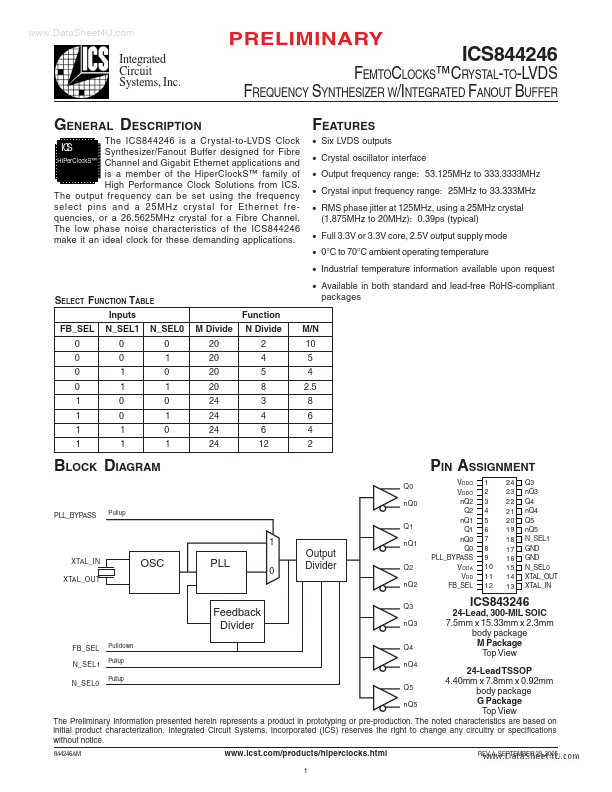
SELECT FUNCTION TABLE
Inputs FB_SEL 0 0 0 0 1 1 1 1 N_SEL1 0 0 1 1 0 0 1 1 N_SEL0 0 1 0 1 0 1 0 1 M Divide 20 20 20 20 24 24 24 24 N Divide 2 4 5 8 3 4 6 12
M/N 10 5 4 2.5 8 6 4 2
BLOCK DIAGRAM
Q0 nQ0 PLL_BYPASS
Pullup
PIN ASSIGNMENT
VDDO VDDO nQ2 Q2 nQ1 Q1 nQ0 Q0 PLL_BYPASS V DDA VDD FB_SEL 1 2 3 4 5 6 7 8 9 10 11 12 24 23 22 21 20 1...
Similar Datasheet