Four Output Differential Buffer
Four Output Differential Buffer for PCIe Gen 1 and Gen 2
DATASHEET
ICS9DB403D
Description
Features/Benefits
The ICS9...
Description
Four Output Differential Buffer for PCIe Gen 1 and Gen 2
DATASHEET
ICS9DB403D
Description
Features/Benefits
The ICS9DB403 is compatible with the Intel DB400v2 Differential Buffer Specification.This buffer provides 4 PCI-Express Gen2 clocks. The ICS9DB403 is driven by a differential output pair from a CK410B+, CK505 or CK509B main clock generator.
Spread spectrum modulation tolerant, 0 to -0.5% down spread and +/- 0.25% center spread.
Supports undriven differential outputs in PD# and SRC_STOP# modes for power management.
Output Features
4 - 0.7V current-mode differential output pairs Supports zero delay buffer mode and fanout mode Bandwidth programming available 50-100 MHz operation in PLL mode 50-400 MHz operation in Bypass mode
Key Specifications
Outputs cycle-cycle jitter < 50ps Outputs skew: 50ps Phase jitter: PCIe Gen1 < 86ps peak to peak Phase jitter: PCIe Gen2 < 3.0/3.1ps rms 28-pin SSOP/TSSOP pacakge Available in RoHS compliant packaging Supports Commercial (0 to +70°C) and Industrial (-40 to
+85°C) temperature ranges
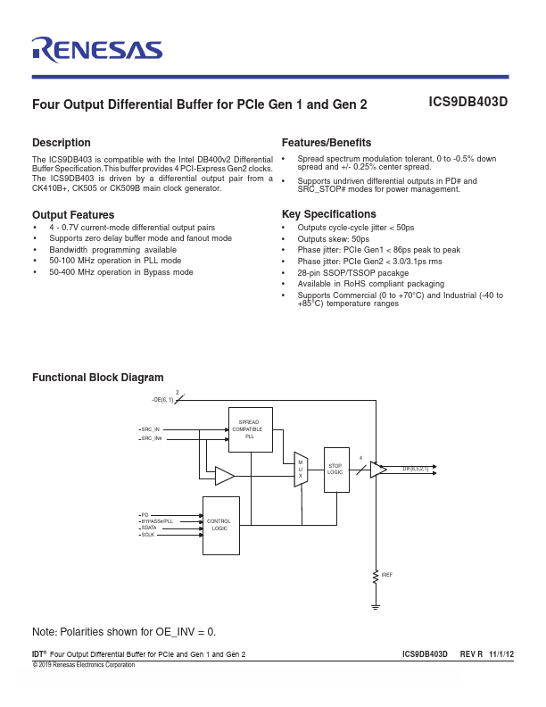
Functional Block Diagram
24 OE-(O6,5E,(26,1, )1)
SRC_IN SRC_IN#
SPREAD COMPATIBLE
PLL
4 M
STOP U LOGIC X
PD BYPASS#/PLL SDATA SCLK
CONTROL LOGIC
DIF(6,5,2,1)
IREF
Note: Polarities shown for OE_INV = 0.
IDT® Four Output Differential Buffer for PCIe and Gen 1 and Gen 2
1
ICS9DB403D REV R 11/1/12
ICS9DB403D Four Output Differential Buffer for PCIe for Gen 1 and Gen 2
Pin Configuration
VDDR 1
28 VDDA
SRC_IN 2...
Similar Datasheet