3.3V ZERO DELAY CLOCK BUFFER
IDT2305B 3.3V ZERO DELAY CLOCK BUFFER
COMMERCIAL AND INDUSTRIAL TEMPERATURE RANGES
3.3V ZERO DELAY CLOCK BUFFER
IDT23...
Description
IDT2305B 3.3V ZERO DELAY CLOCK BUFFER
COMMERCIAL AND INDUSTRIAL TEMPERATURE RANGES
3.3V ZERO DELAY CLOCK BUFFER
IDT2305B
FEATURES:
Phase-Lock Loop Clock Distribution 10MHz to 133MHz operating frequency Distributes one clock input to one bank of five outputs Zero Input-Output Delay Output Skew < 250ps Low jitter <175 ps cycle-to-cycle 50ps typical cycle-to-cycle jitter (15pF, 66MHz) IDT2305B-1 for Standard Drive IDT2305B-1H for High Drive No external RC network required Operates at 3.3V VDD Power down mode Available in SOIC and TSSOP packages
DESCRIPTION:
The IDT2305B is a high-speed phase-lock loop (PLL) clock buffer, designed to address high-speed clock distribution applications. The zero delay is achieved by aligning the phase between the incoming clock and the output clock, operable within the range of 10 to 133MHz.
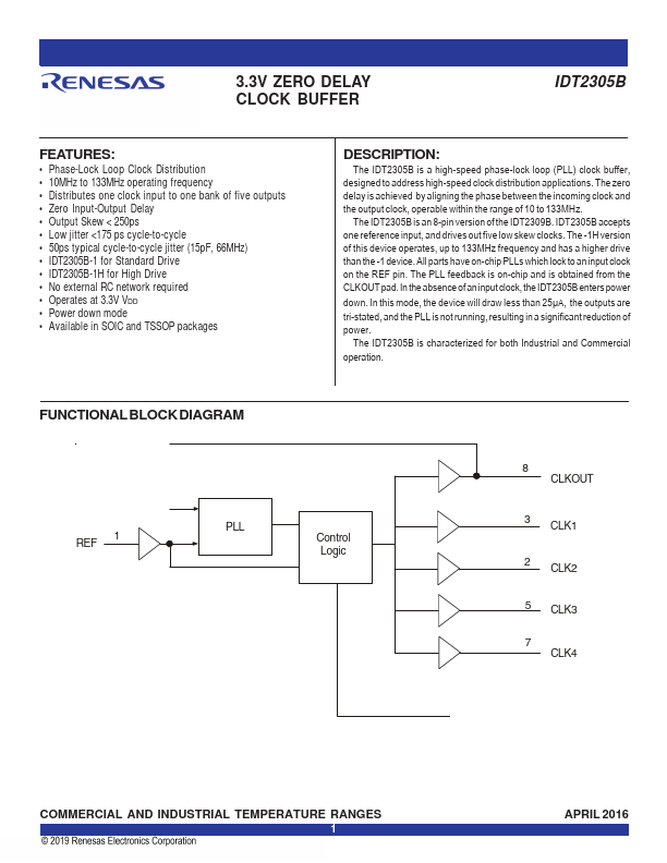
The IDT2305B is an 8-pin version of the IDT2309B. IDT2305B accepts one reference input, and drives out five low skew clocks. The -1H version of this device operates, up to 133MHz frequency and has a higher drive than the -1 device. All parts have on-chip PLLs which lock to an input clock on the REF pin. The PLL feedback is on-chip and is obtained from the CLKOUT pad. In the absence of an input clock, the IDT2305B enters power
down. In this mode, the device will draw less than 25μA, the outputs are
tri-stated, and the PLL is not running, resulting in a significant reduction of power.
The IDT2305B is characterized for both Industria...
Similar Datasheet