3.3V ZERO DELAY CLOCK BUFFER
IDT2308A 3.3V ZERO DELAY CLOCK MULTIPLIER
COMMERCIAL AND INDUSTRIAL TEMPERATURE RANGES
3.3V ZERO DELAY CLOCK MULTIPLIE...
Description
IDT2308A 3.3V ZERO DELAY CLOCK MULTIPLIER
COMMERCIAL AND INDUSTRIAL TEMPERATURE RANGES
3.3V ZERO DELAY CLOCK MULTIPLIER
IDT2308A
FEATURES:
Phase-Lock Loop Clock Distribution for Applications ranging from 10MHz to 133MHz operating frequency
Distributes one clock input to two banks of four outputs Separate output enable for each output bank External feedback (FBK) pin is used to synchronize the outputs
to the clock input Output Skew <200 ps Low jitter <200 ps cycle-to-cycle 1x, 2x, 4x output options (see table):
– IDT2308A-1 1x – IDT2308A-2 1x, 2x – IDT2308A-3 2x, 4x – IDT2308A-4 2x – IDT2308A-1H and -2H for High Drive No external RC network required Operates at 3.3V VDD Available in SOIC and TSSOP packages
DESCRIPTION:
The IDT2308A is a high-speed phase-lock loop (PLL) clock multiplier. It is designed to address high-speed clock distribution and multiplication applications. The zero delay is achieved by aligning the phase between the incoming clock and the output clock, operable within the range of 10 to 133MHz.
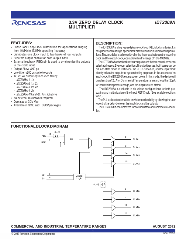
The IDT2308A has two banks of four outputs each that are controlled via two select addresses. By proper selection of input addresses, both banks can be put in tri-state mode. In test mode, the PLL is turned off, and the input clock directly drives the outputs for system testing purposes. In the absence of an input clock, the IDT2308A enters power down. In this mode, the device will
draw less than 12µA for Commercial Temperature range and less t...
Similar Datasheet