CLOCK BUFFER
IDT2309NZ NINE OUTPUT 3.3V CLOCK BUFFER
COMMERCIAL AND INDUSTRIAL TEMPERATURE RANGES
NINE OUTPUT 3.3V CLOCK BUFFER
ID...
Description
IDT2309NZ NINE OUTPUT 3.3V CLOCK BUFFER
COMMERCIAL AND INDUSTRIAL TEMPERATURE RANGES
NINE OUTPUT 3.3V CLOCK BUFFER
IDT2309NZ
FEATURES:
One input to nine output buffer/driver Supports two DIMMs or four SO-DIMMs with one additional
output for feedback to an external or chipset PLL Low power consumption for mobile applications: less than
32mA at 66.6MHz with unloaded outputs 8.7ns input-output delay Buffers all frequencies from DC to 133.33MHz Output-output skew < 250ps Multiple VDD and VSS pins for noise and EMI reduction 3.3V operation High drive capability Available in SOIC and TSSOP packages
DESCRIPTION:
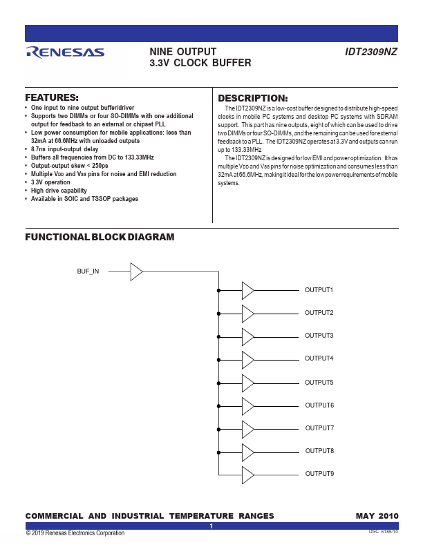
The IDT2309NZ is a low-cost buffer designed to distribute high-speed clocks in mobile PC systems and desktop PC systems with SDRAM support. This part has nine outputs, eight of which can be used to drive two DIMMs or four SO-DIMMs, and the remaining can be used for external feedback to a PLL. The IDT2309NZ operates at 3.3V and outputs can run up to 133.33MHz
The IDT2309NZ is designed for low EMI and power optimization. It has multiple VDD and VSS pins for noise optimization and consumes less than 32mA at 66.6MHz, making it ideal for the low power requirements of mobile systems.
FUNCTIONAL BLOCK DIAGRAM
BUF_IN
OUTPUT1 OUTPUT2 OUTPUT3 OUTPUT4 OUTPUT5 OUTPUT6 OUTPUT7 OUTPUT8 OUTPUT9
COMMERCIAL AND INDUSTRIAL TEMPERATURE RANGES
1
c 2003 Integrated Device Technology, Inc.
MAY 2010
DSC 6189/10
IDT2309NZ NINE OUTPUT 3.3V CLOCK BUFFER
PIN CONFIGURATION
...
Similar Datasheet