3.3 VOLT CMOS SyncBiFIFOTM 16,384 x 36 x 2 32,768 x 36 x 2 65,536 x 36 x 2
IDT72V3682 IDT72V3692 IDT72V36102
FEATURES
...
3.3 VOLT
CMOS SyncBiFIFOTM 16,384 x 36 x 2 32,768 x 36 x 2 65,536 x 36 x 2
IDT72V3682 IDT72V3692 IDT72V36102
FEATURES
Memory storage capacity: IDT72V3682 – 16,384 x 36 x 2 IDT72V3692 – 32,768 x 36 x 2 IDT72V36102 – 65,536 x 36 x 2 Supports clock frequencies up to 100MHz Fast access times of 6.5ns Free-running CLKA and CLKB may be asynchronous or coincident (simultaneous reading and writing of data on a single clock edge is permitted) Two independent clocked FIFOs buffering data in opposite directions
Mailbox bypass register for each FIFO Programmable Almost-Full and Almost-Empty flags Microprocessor Interface Control Logic FFA/IRA, EFA/ORA, AEA, and AFA flags synchronized by CLKA FFB/IRB, EFB/ORB, AEB, and AFB flags synchronized by CLKB Select IDT Standard timing (using EFA, EFB, FFA and FFB flags functions) or First Word Fall Through timing (using ORA, ORB, IRA and IRB flag functions) Available in space-saving 120-pin Thin Quad Flatpack (TQFP) Pin compatible to the lower density parts, IDT72V3622/72V3632/ 72V3642/72V3652/72V3662/72V3672 Industrial temperature range (–40° C to +85°C) is available
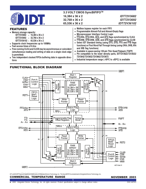
FUNCTIONAL BLOCK DIAGRAM
MBF1 CLKA CSA W/RA ENA MBA Mail 1 Register
Input Register Output Register
Port-A Control Logic
RST1
FIFO1, Mail1 Reset Logic
36
RAM ARRAY 16,384 x 36 32,768 x 36 65,536 x 36
36
Write Pointer
Read Pointer EFB/ORB AEB
FFA/IRA AFA
FIFO 1
Status Flag Logic
FS0 FS1 A0 - A35
16
Programmable Flag Offset Registers
FIFO...