www.DataSheet4U.com
IDT74ALVCH374 3.3V CMOS OCTAL POSITIVE EDGE-TRIGGERED D-TYPE
EXTENDED COMMERCIAL TEMPERATURE RANGE...
www.DataSheet4U.com
IDT74ALVCH374 3.3V
CMOS OCTAL POSITIVE EDGE-TRIGGERED D-TYPE
EXTENDED COMMERCIAL TEMPERATURE RANGE
3.3V
CMOS OCTAL POSITIVE EDGE-TRIGGERED D-TYPE FLIP-FLOP WITH 3-STATE OUTPUTS AND BUS-HOLD
FEATURES:
– – – – – – – – – – 0.5 MICRON
CMOS Technology Typical tSK(o) (Output Skew) < 250ps ESD > 2000V per MIL-STD-883, Method 3015; > 200V using machine model (C = 200pF, R = 0) 1.27mm pitch SOIC, 0.65mm pitch SSOP, 0.635mm pitch QSOP, 0.65mm TSSOP packages Extended commercial range of -40°C to +85°C VCC = 3.3V ±0.3V, Normal Range VCC = 2.7V to 3.6V, Extended Range VCC = 2.5V ±0.2V
CMOS power levels (0.4µ W typ. static) Rail-to-Rail output swing for increased noise margin
IDT74ALVCH374 ADVANCE INFORMATION
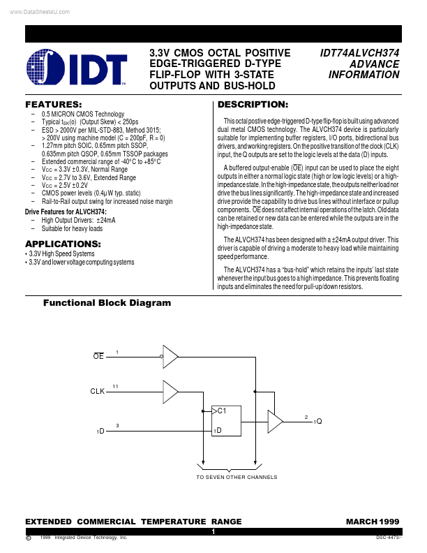
DESCRIPTION:
This octal postive edge-triggered D-type flip-flop is built using advanced dual metal
CMOS technology. The ALVCH374 device is particularly suitable for implementing buffer registers, I/O ports, bidirectional bus drivers, and working registers. On the positive transition of the clock (CLK) input, the Q outputs are set to the logic levels at the data (D) inputs. A buffered output-enable (OE) input can be used to place the eight outputs in either a normal logic state (high or low logic levels) or a highimpedance state. In the high-impedance state, the outputs neither load nor drive the bus lines significantly. The high-impedance state and increased drive provide the capability to drive bus lines without interface or pullup components. OE does not aff...