TECHNICAL DATA
IN74LV174
Hex D-type flip-flop with reset; positive edge-trigger
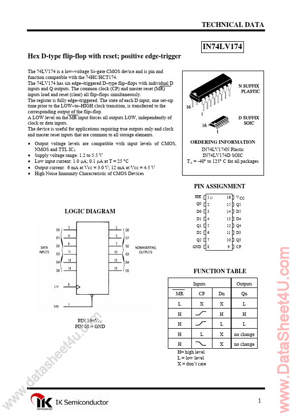
The 74LV174 is a low–voltage Si–gate CM...
TECHNICAL DATA
IN74LV174
Hex D-type flip-flop with reset; positive edge-trigger
The 74LV174 is a low–
voltage Si–gate
CMOS device and is pin and function compatible with the 74HC/HCT174. The 74LV174 has six edge–triggered D–type flip–flops with individual D inputs and Q outputs. The common clock (CP) and master reset (MR) inputs load and reset (clear) all flip–flops simultaneously. The register is fully edge–triggered. The state of each D input, one set–up time prior to the LOW–to–HIGH clock transition, is transferred to the corresponding output of the flip–flop. A LOW level on the MR input forces all outputs LOW, independently of clock or data inputs. The device is useful for applications requiring true outputs only and clock and master reset inputs that are common to all storage elements. Output
voltage levels are compatible with input levels of
CMOS, NMOS and TTL ICS Supply
voltage range: 1.2 to 5.5 V Low input current: 1.0 µА; 0.1 µА at Т = 25 °С Output current: 6 mA at Vcc = 3.0 V; 12 mA at Vcc = 4.5 V High Noise Immunity Characteristic of
CMOS Devices ORDERING INFORMATION IN74LV174N Plastic IN74LV174D SOIC TA = -40° to 125° C for all packages
PIN ASSIGNMENT
MR Q0 1 2 3 4 5 6 7 8 16 15 14 13 12 11 10 9 V CC Q5 D5 D4 Q4 D3 Q3
LOGIC DIAGRAM
D0 D1 Q1 D2 Q2 GND
FUNCTION TABLE
CP
Inputs MR CP X Dn X H L L X X
Outputs Qn L H L no change no change
MR
L PIN 16=VCC PIN 08 = GND
w
w
w
.d
e e h s a t a
. u t4
m o c
H H H H H= high level L = low level X = d...