TECHNICAL DATA
IN74LV241
OCTAL BUFFER/LINE DRIVE; 3-STATE
The IN74LV241 is a low-voltage Si-gate CMOS device and is pin...
TECHNICAL DATA
IN74LV241
OCTAL BUFFER/LINE DRIVE; 3-STATE
The IN74LV241 is a low-
voltage Si-gate
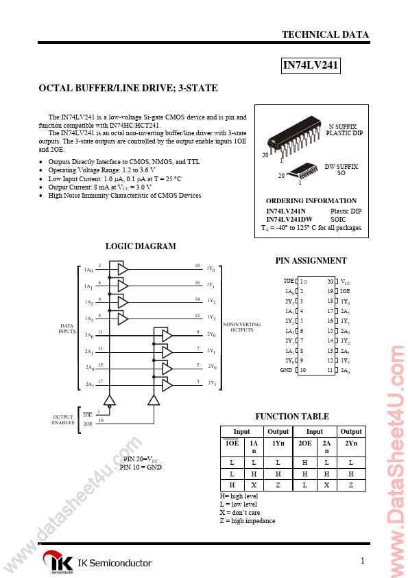
CMOS device and is pin and function compatible with IN74HC/HCT241. The IN74LV241 is an octal non-inverting buffer/line driver with 3-state outputs. The 3-state outputs are controlled by the output enable inputs 1OE and 2OE. Outputs Directly Interface to
CMOS, NMOS, and TTL Operating
Voltage Range: 1.2 to 3.6 V Low Input Current: 1.0 µA, 0.1 µА at Т = 25 °С Output Current: 8 mA at VCC = 3.0 V High Noise Immunity Characteristic of
CMOS Devices
N SUFFIX PLASTIC DIP
20
1 20 1
DW SUFFIX SO
ORDERING INFORMATION IN74LV241N Plastic DIP IN74LV241DW SOIC TA = -40° to 125° C for all packages
LOGIC DIAGRAM
1A0 1A1 1A2 1A3 DATA INPUTS 2A0 2A1 2 4 6 8 11 13 18 16 14 12 9 7 5 3 1Y0 1Y1 1Y2 1Y3 2Y0 2Y1 2Y0 2Y1 NONINVERTING OUTPUTS
PIN ASSIGNMENT
1OE 1A0 2Y3 1A1 2Y2 1A2 2Y1 1A3 2Y0 GND 1 2 3 4 5 6 7 8 9 10 20 19 18 17 16 15 14 13 12 11 VCC 2OE 1Y0 2A3 1Y1 2A2 2A1 1Y3 2A0 1Y2
2A0 15 2A1 17
OUTPUT ENABLES
1OE 2OE
1 19
FUNCTION TABLE
Input Output 1Yn L H Z Input 2OE H H L 2A n L H X Output 2Yn L H Z
w
w
a d . w
e h s a t
4 t e
c . u
PIN 20=VCC PIN 10 = GND
om
1OE L L H
1A n L H X
H= high level L = low level X = don’t care Z = high impedance
1
www.DataSheet4U.com
IN74LV241
MAXIMUM RATINGS*
Symbol VCC IIK * IO * ICC IGND PD
1 2
Parameter DC supply
voltage DC Input diode current DC Output diode current DC Output source or sink current DC VCC current DC GND current ...